Absolute maximum ratings, t, 25°c unless otherwise specified, Inverter sector – C&H Technology CM150DX-24A User Manual
Page 3
CM150DX-24A
Dual IGBTMOD™ NX-Series Module
150 Amperes/1200 Volts
Powerex, Inc., 173 Pavilion Lane, Youngwood, Pennsylvania 15697 (724) 925-7272
2
Rev. 3/09
Absolute Maximum Ratings,
T
j
= 25°C unless otherwise specified
Characteristics
Symbol
CM150DX-24A
Units
Power Device Junction Temperature
T
j
-40 to 150
°C
Storage Temperature
T
stg
-40 to 125
°C
Mounting Torque, M5 Mounting Screws
—
31
in-lb
Mounting Torque, M6 Main Terminal Screws
—
40
in-lb
Module Weight (Typical)
—
330
Grams
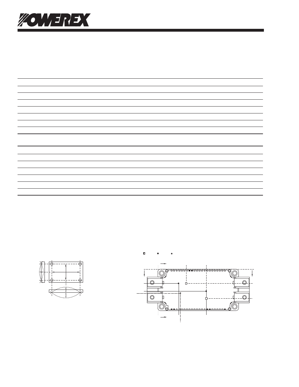
Baseplate Flatness, On Centerline X, Y (See Below)
—
±0 ~ +100
µm
Isolation Voltage, AC 1 minute, 60Hz Sinusoidal
V
ISO
2500
Volts
Inverter Sector
Collector-Emitter Voltage (G-E Short)
V
CES
1200
Volts
Gate-Emitter Voltage (C-E Short)
V
GES
±20
Volts
Collector Current (T
C
= 91°C)
*1
I
C
150
Amperes
Peak Collector Current (Pulse)
*3
I
CM
300
Amperes
Emitter Current (T
C
= 25°C)
*1*4
I
E
*2
150
Amperes
Peak Emitter Current (Pulse)
*3
I
EM
*2
300
Amperes
Maximum Collector Dissipation (T
C
= 25°C)
*1*4
P
C
960
Watts
*1 Case temperature (T
C
) and heatsink temperature (T
f
) are defined on the surface of the baseplate and heatsink at just under the chip.
*2 I
E
, I
EM
, V
EC
, t
rr
and Q
rr
represent ratings and characteristics of the anti-parallel, emitter-to-collector free-wheel diode (FWDi).
*3 Pulse width and repetition rate should be such that device junction temperature (T
j
) does not exceed T
j(max)
rating.
*4 Junction temperature (T
j
) should not increase beyond T
j(max)
rating.
1
2
3 4 5
6
7 8
9 10 11 12 13 14 15 16 17 18 19 20 21 22
23
24
48
47
46 45 44 43 42 41 40 39 38 37 36 35 34 33 32 31 30 29 28 27 26 25
0
0
0
Dimensions in mm (Tolerance: ±1mm)
IGBT FWDi NTC Thermistor
Chip Location (Top View)
0
21.2
32.6
31
.3
73.5
21.2
42.5
73.5
43.8
34.2
36.2
Th
CHIP LOCATION (TOP VIEW)
BASEPLATE FLATNESS
MEASUREMENT POINT
HEATSINK SIDE
– :
CONC
A
VE
+ :
CONVEX
– : CONCAVE
X
Y
+ : CONVEX
HEA
TSINK SIDE