Vsk.105..pbf series, Vishay high power products, Thyristor/diode and thyristor/thyristor (add-a-pak – C&H Technology VSK.105..PbF Series User Manual
Page 3: Generation 5 power modules), 105 a, Electrical specifications, Voltage ratings, On-state conduction
www.vishay.com
For technical questions, contact: [email protected]
Document Number: 94416
2
Revision: 04-Jul-08
VSK.105..PbF Series
Vishay High Power Products
Thyristor/Diode and Thyristor/Thyristor
(ADD-A-PAK
TM
Generation 5 Power Modules), 105 A
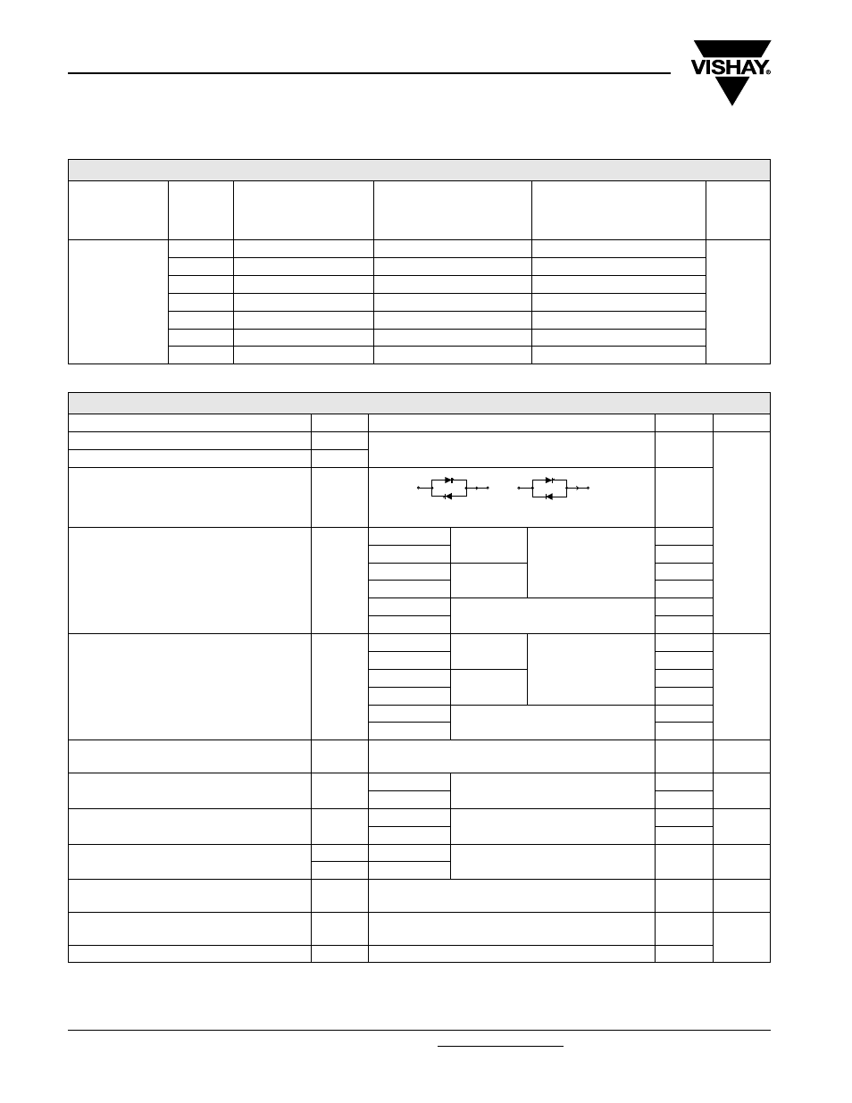
ELECTRICAL SPECIFICATIONS
Notes
(1)
I
2
t for time t
x
= I
2
√t x √t
x
(2)
Average power = V
T(TO)
x I
T(AV)
+ r
t
x (I
T(RMS)
)
2
(3)
16.7 % x
π x I
AV
< I <
π x I
AV
(4)
I>
π x I
AV
VOLTAGE RATINGS
TYPE NUMBER
VOLTAGE
CODE
V
RRM
, MAXIMUM
REPETITIVE PEAK
REVERSE VOLTAGE
V
V
RSM
, MAXIMUM
NON-REPETITIVE PEAK
REVERSE VOLTAGE
V
V
DRM
, MAXIMUM REPETITIVE
PEAK OFF-STATE VOLTAGE,
GATE OPEN CIRCUIT
V
I
RRM,
I
DRM
AT 130 °C
mA
IRK.105
04
400
500
400
20
06
600
700
600
08
800
900
800
10
1000
1100
1000
12
1200
1300
1200
14
1400
1500
1400
16
1600
1700
1600
ON-STATE CONDUCTION
PARAMETER
SYMBOL
TEST CONDITIONS
VALUES
UNITS
Maximum average on-state current (thyristors)
I
T(AV)
180° conduction, half sine wave,
T
C
= 85 °C
105
A
Maximum average forward current (diodes)
I
F(AV)
Maximum continuous RMS on-state current,
as AC switch
I
O(RMS)
235
Maximum peak, one-cycle non-repetitive
on-state or forward current
I
TSM
or
I
FSM
t = 10 ms
No voltage
reapplied
Sinusoidal
half wave,
initial T
J
= T
J
maximum
1785
t = 8.3 ms
1870
t = 10 ms
100 % V
RRM
reapplied
1500
t = 8.3 ms
1570
t = 10 ms
T
J
= 25 °C, no voltage reapplied
2000
t = 8.3 ms
2100
Maximum I
2
t for fusing
I
2
t
t = 10 ms
No voltage
reapplied
Initial T
J
= T
J
maximum
15.91
kA
2
s
t = 8.3 ms
14.52
t = 10 ms
100 % V
RRM
reapplied
11.25
t = 8.3 ms
10.27
t = 10 ms
T
J
= 25 °C, no voltage reapplied
20.00
t = 8.3 ms
18.30
Maximum I
2
√t for fusing
I
2
√t
(1)
t = 0.1 to 10 ms, no voltage reapplied
T
J
= T
J
maximum
159.1
kA
2
√s
Maximum value or threshold voltage
V
T(TO)
(2)
Low level
(3)
T
J
= T
J
maximum
0.80
V
High level
(4)
0.85
Maximum value of on-state
slope resistance
r
t
(2)
Low level
(3)
T
J
= T
J
maximum
2.37
m
Ω
High level
(4)
2.25
Maximum peak on-state or forward voltage
V
TM
I
TM
=
π x I
T(AV)
T
J
= 25 °C
1.64
V
V
FM
I
FM
=
π x I
F(AV)
Maximum non-repetitive rate of rise of
turned on current
dI/dt
T
J
= 25 °C, from 0.67 V
DRM
,
I
TM
=
π x I
T(AV)
, I
g
= 500 mA, t
r
< 0.5 µs, t
p
> 6 µs
150
A/µs
Maximum holding current
I
H
T
J
= 25 °C, anode supply = 6 V,
resistive load, gate open circuit
250
mA
Maximum latching current
I
L
T
J
= 25 °C, anode supply = 6 V, resistive load
400
or
I
(RMS)
I
(RMS)