Vsku/v41, 56..pbf series, Vishay high power products, Thyristor/thyristor, 45/60 a (add-a-pak – C&H Technology VSKU-V56..PbF Series User Manual
Page 4: Generation 5 power modules)
Document Number: 94515
For technical questions, contact: [email protected]
www.vishay.com
Revision: 25-Apr-08
3
VSKU/V41, 56..PbF Series
Thyristor/Thyristor, 45/60 A
(ADD-A-PAK
TM
Generation 5 Power Modules)
Vishay High Power Products
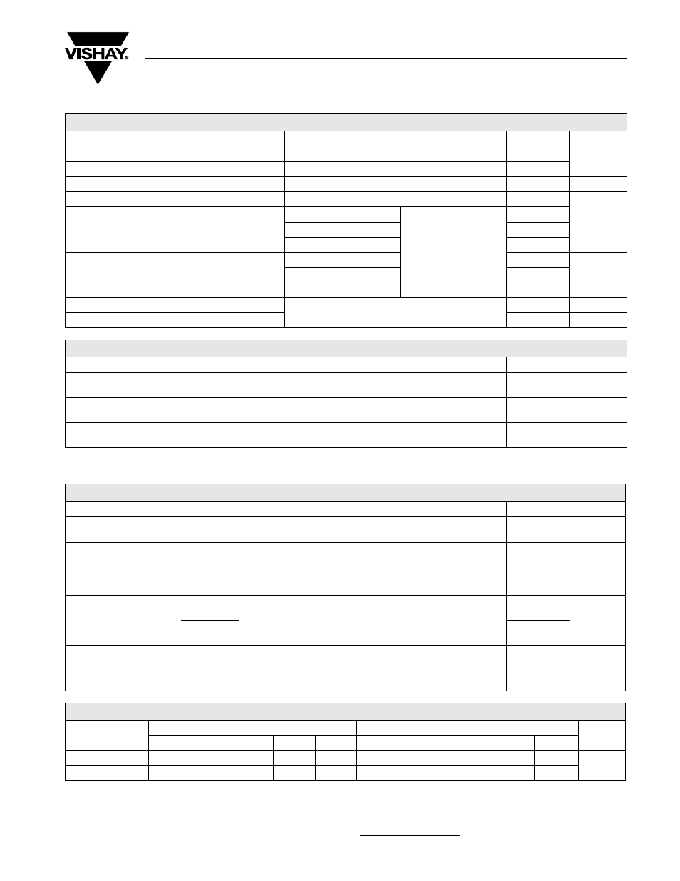
Note
(1)
Available with dV/dt = 1000 V/µs, to complete code add S90 i.e. VSKU41/16AS90
Note
• Table shows the increment of thermal resistance R
thJC
when devices operate at different conduction angles than DC
TRIGGERING
PARAMETER
SYMBOL
TEST CONDITIONS
VALUES
UNITS
Maximum peak gate power
P
GM
10
W
Maximum average gate power
P
G(AV)
2.5
Maximum peak gate current
I
GM
2.5
A
Maximum peak negative gate voltage
- V
GM
10
V
Maximum gate voltage required to trigger
V
GT
T
J
= - 40 °C
Anode supply = 6 V
resistive load
4.0
T
J
= 25 °C
2.5
T
J
= 125 °C
1.7
Maximum gate current required to trigger
I
GT
T
J
= - 40 °C
270
mA
T
J
= 25 °C
150
T
J
= 125 °C
80
Maximum gate voltage that will not trigger
V
GD
T
J
= 125 °C, rated V
DRM
applied
0.25
V
Maximum gate current that will not trigger
I
GD
6
mA
BLOCKING
PARAMETER
SYMBOL
TEST CONDITIONS
VALUES
UNITS
Maximum peak reverse and off-state
leakage current at V
RRM
, V
DRM
I
RRM,
I
DRM
T
J
= 125 °C, gate open circuit
15
mA
RMS insulation voltage
V
INS
50 Hz, circuit to base, all terminals shorted
2500 (1 min)
3500 (1 s)
V
Maximum critical rate of rise of
off-state voltage
dV/dt
(1)
T
J
= 125 °C, linear to 0.67 V
DRM
, gate open circuit
500
V/µs
THERMAL AND MECHANICAL SPECIFICATIONS
PARAMETER
SYMBOL
TEST CONDITIONS
VALUES
UNITS
Junction operating and storage
temperature range
T
J
, T
Stg
- 40 to 125
°C
Maximum internal thermal resistance,
junction to case per module
R
thJC
DC operation
0.23
K/W
Typical thermal resistance,
case to heatsink
R
thCS
Mounting surface, flat, smooth and greased
0.1
Mounting torque ± 10 %
to heatsink
A mounting compound is recommended and the
torque should be rechecked after a period of 3 hours
to allow for the spread of the compound.
5
Nm
busbar
3
Approximate weight
110
g
4
oz.
Case style
JEDEC
TO-240AA
ΔR CONDUCTION PER JUNCTION
DEVICES
SINE HALF WAVE CONDUCTION
RECTANGULAR WAVE CONDUCTION
UNITS
180°
120°
90°
60°
30°
180°
120°
90°
60°
30°
VSKU/V41
0.11
0.13
0.17
0.23
0.34
0.09
0.14
0.18
0.23
0.34
°C/W
VSKU/V56
0.09
0.11
0.13
0.18
0.27
0.07
0.11
0.14
0.19
0.28