Mounting instructions for add-a-pak generation vii, Vishay semiconductors – C&H Technology VSKDS440-030 User Manual
Page 9

Mounting Instructions for
ADD-A-PAK Generation VII
www.vishay.com
For technical questions, contact:
Document Number: 95043
2
Revision: 17-Dec-08
Application Note
Vishay Semiconductors
APPLICATI
O
N NOTE
Next, make a uniform coating on the heatsink mounting
surfaces and module substrate with a good quality thermal
compound. Screen printing of the compound is
recommended, as well as direct application through a roller
or spatula. The datasheet values for thermal resistance
assume a uniform layer of thermal compound with a
maximum thickness of 0.08 mm. The thermal conductivity of
the compound should be no less than 0.5 W/mK. Apply
uniform pressure on the package to force the compound to
spread over the entire contact area, and check the device
bottom surface to verify full and uniform coverage.
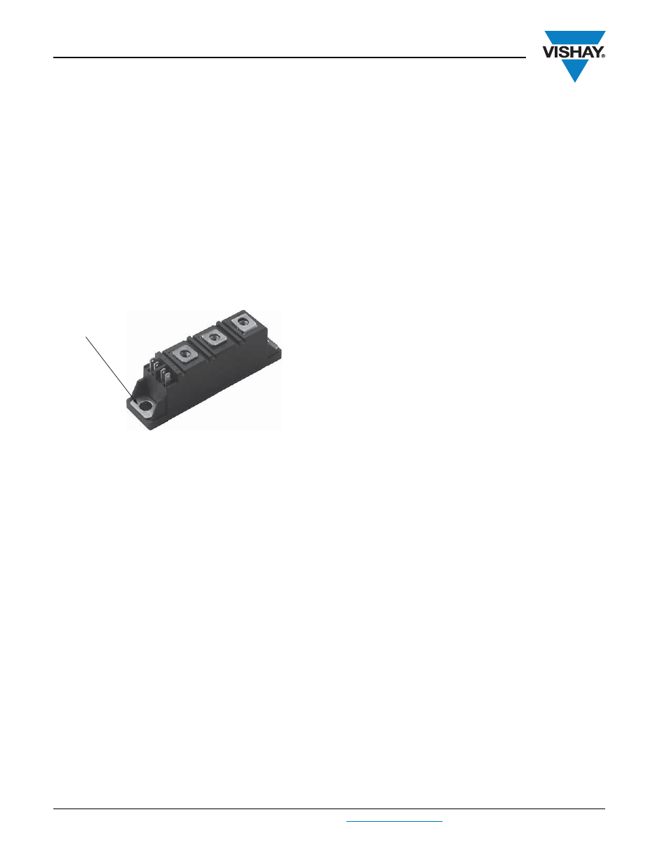
Bolt the module to the heatsink using the two fixing holes.
An even amount of torque should be applied for each
individual mounting screw. An M6 screw should be used
with lock washers. A torque wrench, which is accurate in the
specified range, must be used in mounting the module to
achieve optimum results. The first mounting screw should
be tightened to one third of the recommended torque; the
second screw should then be tightened to the same torque.
Full tightening of both the screws can then be completed by
applying the recommended torque (see data in bulletins).
Over-tightening the mounting screw may lead to
deformation of the package, which would hence increase
the thermal resistance and damage the semiconductors.
After a period of three hours, check the torque with a final
tightening in opposite sequence to allow the spread of the
compound.
Power terminals can be screwed to busbars and/or flexible
cables with eyelets.
We recommend the use of M5 screws with spring washers.
Users should consult published datasheets to determine the
optimal torque.
AAP Generation VII modules are designed to guarantee a
good and reliable contact even at 3 ± 10 % Nm on a busbar,
so there is no need to apply an especially high level of force
to obtain a good and reliable connection.
SOLDERING TO THE PCB
The signal terminal (gate and auxiliary cathode) pins of AAP
Gen VII modules based on thyristors can be soldered to the
PCB using hand iron or wave soldering processes.
The PCB should be designed with appropriate tolerances on
the hole diameters, and soldering must be done without
imposing any mechanical stress on the module pins (pulling
and tensioning the pins).
To prevent overheating of the device, the soldering time
should not exceed 8 s to 10 s at a temperature of 260 °C.
Alternatively, a fast-on cable connector can be used to
contact the signal pins.
