Vishay semiconductors, Electrical specifications (t, Switching characteristics (t – C&H Technology VS-EMG050J60N User Manual
Page 3
VS-EMG050J60N
www.vishay.com
Vishay Semiconductors
Revision: 09-Dec-11
2
Document Number: 93495
For technical questions within your region:
,
,
THIS DOCUMENT IS SUBJECT TO CHANGE WITHOUT NOTICE. THE PRODUCTS DESCRIBED HEREIN AND THIS DOCUMENT
ARE SUBJECT TO SPECIFIC DISCLAIMERS, SET FORTH AT
www.vishay.com/doc?91000
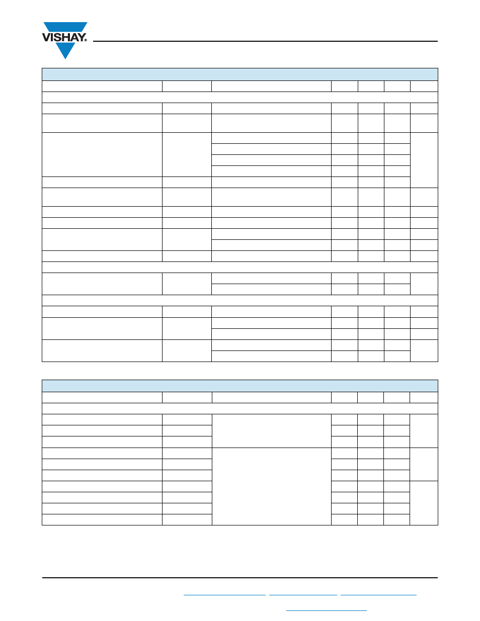
ELECTRICAL SPECIFICATIONS (T
J
= 25 °C unless otherwise noted)
PARAMETER
SYMBOL
TEST CONDITIONS
MIN.
TYP.
MAX.
UNITS
PFC IGBT Q1 - Q2
Collector to emitter breakdown voltage
BV
CES
V
GE
= 0 V, I
C
= 500 μA
600
-
-
V
Temperature coefficient of
breakdown voltage
BV
CES
/
T
J
V
GE
= 0 V, I
C
= 500 μA
(25 °C to 125 °C)
-
0.1
-
V/°C
Collector to emitter voltage
V
CE(ON)
V
GE
= 15 V, I
C
= 27 A
-
1.44
1.75
V
V
GE
= 15 V, I
C
= 50 A
-
1.8
2.1
V
GE
= 15 V, I
C
= 27 A, T
J
= 125 °C
-
1.7
2.05
V
GE
= 15 V, I
C
= 50 A, T
J
= 125 °C
-
2.2
2.5
Gate threshold voltage
V
GE(th)
V
CE
= V
GE
, I
C
= 250 μA
2.9
3.9
5.3
Temperature coefficient of threshold
voltage
V
GE(th)
/
T
J
V
CE
= V
GE
, I
C
= 1 mA
( 25 °C to 125 °C)
-
- 10
-
mV/°C
Forward transconductance
g
fe
V
CE
= 20 V, I
C
= 50 A
-
95
-
s
Transfer characteristics
V
GE
V
CE
= 20 V, I
C
= 50 A
-
5.9
-
V
Zero gate voltage collector current
I
CES
V
GE
= 0 V, V
CE
= 600 V
-
3
100
μA
V
GE
= 0 V, V
CE
= 600 V, T
J
= 125 °C
-
0.170
3
mA
Gate to emitter leakage current
I
GES
V
GE
= ± 20 V, V
CE
= 0 V
-
± 200
nA
ANTIPARALLEL DIODE D1 - D2
Forward voltage drop
V
F
I
F
= 20 A
-
2.19
2.4
V
I
F
= 20 A, T
J
= 125 °C
-
1.93
2.15
PFC DIODE D3 - D4
Cathode to anode breakdown voltage
V
BR
I
R
= 500 μA
600
-
-
V
Reverse leakage current
I
RM
V
R
= 600 V
-
27
250
μA
V
R
= 600 V, T
J
= 125 °C
-
0.1
1
mA
Forward voltage drop
V
F
I
F
= 10 A
-
1.34
1.63
V
I
F
= 10 A, T
J
= 125 °C
-
1.36
1.65
SWITCHING CHARACTERISTICS (T
J
= 25 °C unless otherwise noted)
PARAMETER
SYMBOL
TEST CONDITIONS
MIN.
TYP.
MAX.
UNITS
PFC IGBT Q1 - Q2 (WITH FREEWHEELING D3 - D4 PFC DIODE)
Total gate charge (turn-on)
Q
g
I
C
= 70 A
V
CC
= 400 V
V
GE
= 15 V
-
480
720
nC
Gate to emitter charge (turn-on)
Q
ge
-
82
164
Gate to collector charge (turn-on)
Q
gc
-
160
260
Turn-on switching loss
E
ON
I
C
= 50 A
V
CC
= 400 V
V
GE
= 15 V
R
g
= 4.7
L = 500 μH
T
J
= 25 °C
(1)
-
0.155
-
mJ
Turn-off switching loss
E
OFF
-
0.471
-
Total switching loss
E
TOT
-
0.626
-
Turn-on delay time
t
d(on)
-
196
-
ns
Rise time
t
r
-
29
-
Turn-off delay time
t
d(off)
-
220
-
Fall time
t
f
-
67
-