Vsk.26..pbf series, Vishay high power products, Thyristor/diode and thyristor/thyristor (add-a-pak – C&H Technology VSK.26..PbF Series User Manual
Page 7: Generation 5 power modules), 27 a
www.vishay.com
For technical questions, contact: [email protected]
Document Number: 94418
6
Revision: 22-Apr-08
VSK.26..PbF Series
Vishay High Power Products
Thyristor/Diode and Thyristor/Thyristor
(ADD-A-PAK
TM
Generation 5 Power Modules), 27 A
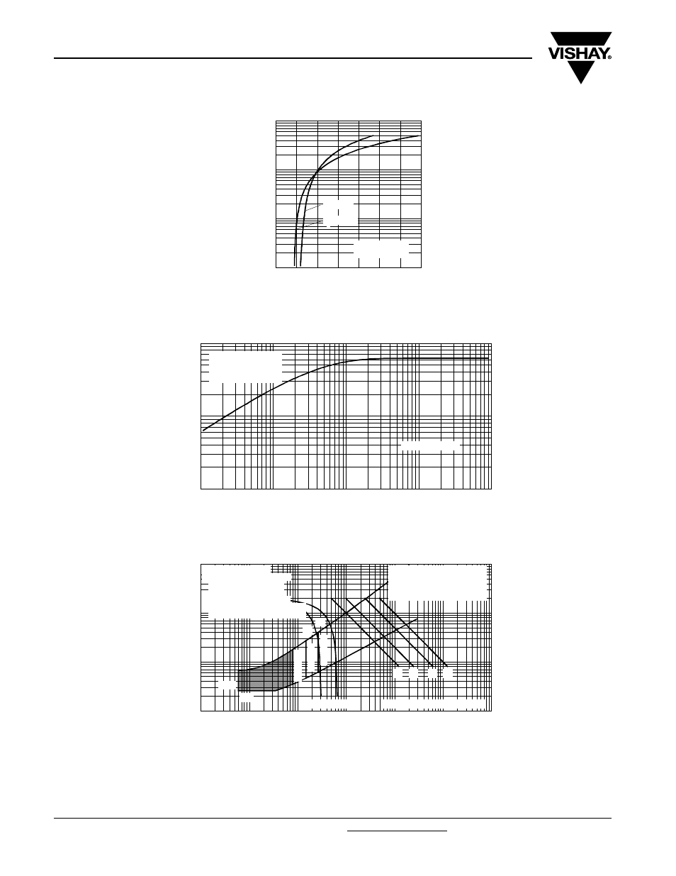
Fig. 10 - On-State Voltage Drop Characteristics
Fig. 11 - Thermal Impedance Z
thJC
Characteristics
Fig. 12 - Gate Characteristics
1
10
100
1000
0
1
2
3
4
5
6
7
T = 25°C
J
In
st
a
n
ta
n
e
o
u
s O
n
-s
ta
te
C
u
rr
e
n
t (
A
)
Instantaneous On-state Voltage (V)
T = 125°C
J
VSK.26.. Series
Per Junction
0.01
0.1
1
0.001
0.01
0.1
1
10
Square Wave Pulse Duration (s)
Steady State Value:
R = 0.62 K/ W
(DC Operation)
thJC
th
J
C
Tr
an
si
e
n
t
T
h
er
m
a
l I
m
pe
dan
c
e
Z
(K
/W
)
VSK.26.. Series
0.1
1
10
100
0.001
0.01
0.1
1
10
100
1000
(b )
(a)
Rectangular gate pulse
(4) (3)
(2) (1)
(1) PGM = 100 W, tp = 500 µs
(2) PGM = 50 W, tp = 1 ms
(3) PGM = 20 W, tp = 25 ms
(4) PGM = 10 W, tp = 5 ms
Instantaneous Gate Current (A)
In
st
a
n
ta
n
e
o
u
s G
a
te
V
o
lt
ag
e (
V
)
TJ =
-
4
0
°
C
TJ =
2
5
°
C
TJ
=
1
2
5
°
C
a)Rec ommended load line for
b)Rec ommended load line for
VGD
IGD
Frequenc y Limited by PG(AV)
rated di/ dt: 20 V, 30 ohms
tr = 0.5 µs, tp >= 6 µs
<= 30% rated d i/ dt: 20 V, 65 ohms
tr = 1 µs, tp >= 6 µs
VSK.26.. Series