Protection function timing diagrams – C&H Technology PS21963-4ES User Manual
Page 8
PS21963-4ES
Intellimod™ Module
Dual-In-Line Intelligent Power Module
8 Amperes/600 Volts
Powerex, Inc., 173 Pavilion Lane, Youngwood, Pennsylvania 15697 (724) 925-7272
7
Rev. 12/09
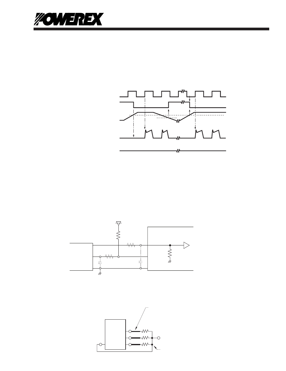
Protection Function Timing Diagrams
C1
C4
C5
C2
UVDt
C6
C3
SET
RESET
RESET
HIGH LEVEL (NO FAULT OUTPUT)
UVDBr
CONTROL INPUT
PROTECTION
CIRCUIT STATE
CONTROL SUPPLY
VOLTAGE VDB
OUTPUT CURRENT IC
FAULT OUTPUT FO
Under-Voltage Protection (Upper-side, UVDB)
C1: Control supply voltage rises – After the voltage level reaches UVDBr, the drive circuit begins to work
at the rising edge of the next input signal.
C2: Normal operation – IGBT turn on and conducting current.
C3: Under-voltage trip (UVDBt).
C4: IGBT stays off regardless of the control input level, but there is no FO signal output.
C5: Under-voltage reset (UVDr).
C6: Normal operation – IGBT turn on and conducting current.
Typical Interface Circuit
Wiring Method Around Shunt Resistor
VNC
NW
NV
NU
DIP-IPM
Wiring inductance should be less than 10nH.
(Equivalent to the inductance of a copper pattern with
length = 17mm, width = 3mm, and thickness = 100
µ
m.)
Shunt
Resistors
Please make the connection of shunt resistor
close to VNC terminal.
UP, VP, WP, UN, VN, WN
MCU
5V LINE
10kΩ
3.3kΩ (MIN)
FO
VNC (LOGIC)
DIP-IPM
NOTE: RC coupling at each input
(parts shown dotted) may change
depending on the PWM control
scheme used in the application and
the wiring impedance of the printed
circuit board. The DIP-IPM input signal
section integrates a 3.3kΩ (min)
pull-down resistor. Therefore, when
using an external filtering resistor, care
must be taken to satisfy the turn-on
threshold voltage requirement.