Application circuit – C&H Technology PS22A74 User Manual
Page 6
PS22A74
Intellimod™ Module
Dual-In-Line Intelligent Power Module
15 Amperes/1200 Volts
Powerex, Inc., 173 Pavilion Lane, Youngwood, Pennsylvania 15697 (724) 925-7272
5
Rev. 08/09
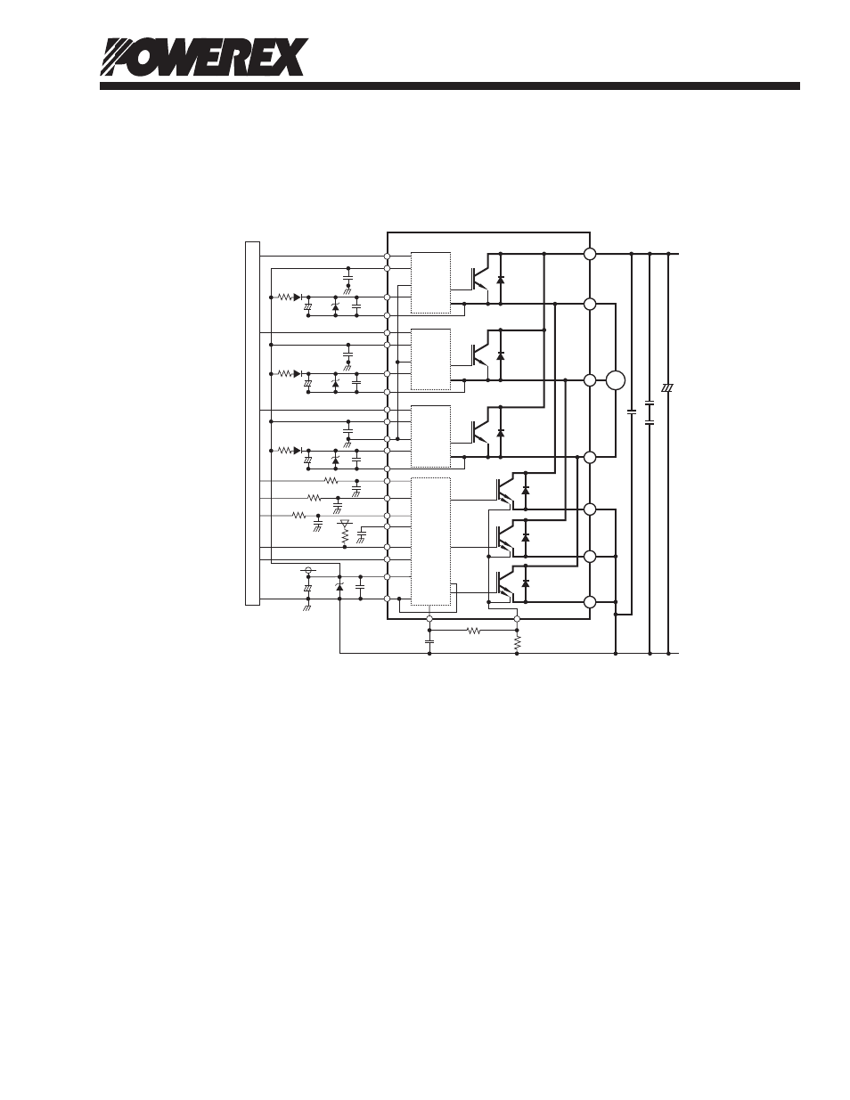
Application Circuit
Component Selection:
Dsgn.
Typ. Value
Description
D1
1A, 600V
Control and boot strap supply overvoltage suppression
DZ1
24V, 1W
Control and boot strap supply over voltage suppression
C1
10-100µF, 50V
Boot strap supply reservoir – electrolytic long lifem low impedance, 105°C
C2
0.22-2.0µF, 50V
Local decoupling/High frequency noise filters – multilayer ceramic (Note 4)
C3
200 to 2500µF, 450V
Main DC bus filter capacitor – electrolytic, long life, high ripple current, 105°C
C4
100pF, 50V
Optional input signal noise filter – multilayer ceramic (Note 11)
C5
0.1-0.22µF, 1000V
Surge voltage suppression (Note 2)
CSF
1000pF, 50V
Short circuit detection filter capacitor – multilayer ceramic
RSF
1.8kΩ
Short circuit detection filter resistor
RSHUNT 20ohm-500ohm
Current sensing resistor
R1
1-10Ω
Boot strap supply inrush limiting resistor – non-inductive, temperature stable, tight tolerance (Note 5)
R2
330Ω
Optional input signal noise filter (Note 11)
R3
10kΩ
Fault signal pull-up resistor (Note 9)
Notes:
1) If control GND is connected to power GND by broad pattern, it may cause malfunction by power GND fluctuation.
It is recommended to connect control GND at only a point at which NU, NV, NW are connected to power GND line.
2) To prevent surge destruction, the wiring between the smoothing capacitor and the P-N1 terminals should be as short as
possible. Generally inserting a 0.1µ ~ 0.22µF snubber capacitor C3 between the P-N1 terminals is recommended.
3) The time constant R1,C4 of RC filter for preventing the protection circuit malfunction should be selected in the range of 1.5µ ~ 2µs.
SC interrupting time might vary with the wiring pattern. Tight tolerance, temp-compensated type is recommended for R1,C4.
4) All capacitors should be mounted as close to the terminals of the DIPIPM as possible. (C1: good temperature, frequency
characteristics electrolytic type, and C2 : good temperature, frequency and DC bias characteristic ceramic type are recommended.)
5) It is recommended to insert a Zener diode DZ1 (24V/1W) between each pair of control supply terminals to prevent surge destruction.
6) To prevent erroneous SC protection, the wiring from VSC terminals to CIN filter should be divided at the point D that is close
to the terminal of sense resistor and the wiring should be patterned as short as possible.
7) For sense resistor, the variation within 1% (including temperature characteristics), low inductance type is recommended.
1/8W is recommended, but an evaluation of your system is recommended.
8) To prevent erroneous operation, wiring A, B, and C should be as short as possible.
9) FO output is open drain type. It should be pulled up to the positive side of 5V or 15V power supply with a resistor that limits
FO sink current (IFO) under 1mA. (Over 5.1kΩ is needed and 10kΩ is recommended for 5V supply.)
10) Error signal output width (tFO) can be set by the capacitor connected to the CFO terminal. tFO(typ) = CFO / 9.1 x 10⁻⁶ (s).
11) Input drive is high-active type. There is a 3.3kΩ pull-down resistor integrated in the IC input circuit. To prevent malfunction, the wiring of each input
should be patterned as short as possible. When inserting the RC filter, make sure the input signal level meets the turn-on and turn-off threshold voltage.
Thanks to HVIC inside the module, connection to the MCU may be direct or with an opto-coupler.
VN1
UN
FO
VOT
VNC
VNO
VSC
D
B
C
A
RSHUNT
CIN
CSF
RSF
VN
WN
CFO
HVIC1
IGBT1
FWDi1
IGBT2
FWDi2
IGBT3
IGBT4
IGBT5
IGBT6
FWDi3
FWDi4
FWDi5
FWDi6
LVIC
P
U
HVIC2
V
VWFB
VP1
VWFS
WP
VPC
HVIC3
W
NU
NV
NW
C2
DZ1
C1
VD
15V
+
+
C2
C4
C4
C4
R3
R2
R2
R2
C2
DZ1
C1
D1
+
VVFB
VP1
VVFS
VP
C2
C2
DZ1
C1
D1
MCU
+
VUFB
VP1
VUFS
UP
C2
C2
C3
C3
C5
DZ1
C1
D1
+
M