VXI SM8000 User Manual
Page 40
VXI Technology, Inc.
40
SM8000 Series Programming
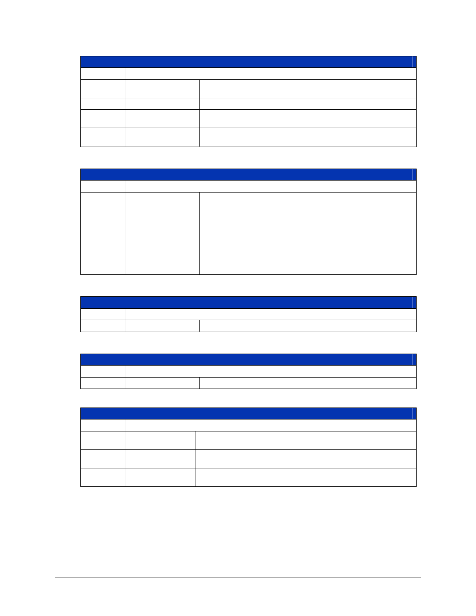
Control Register – Write Only
ADDR
Plug-In LA+0x04
D15 A24/A32
Enable
1 = write a 1 to this bit to enable A24/A32 memory access
0 = to disable access
D14-D2
Reserved
Writes to these bits have no effect.
D1 Sysfail
Inhibit
Write a 1 to this bit to prevent the module from asserting the
SYSFAIL* line.
D0 Reset
1 = write a 1 to this bit to force the module into a reset state
0 = write a 0 to release the reset state
Offset Register – Read and Write
ADDR
Plug-In LA+0x06
D15-D0
A24/A32 Memory
Offset
The value written to this 16-bit register, times 256, sets the base
address of the A24 memory space used by the module. The value
written to this 16-bit register, times 65,536, sets the base address
of the A32 memory space used by the module. A read from this
register reflects the previously written value. Because of the
required memory size, bits D4-D0 are disregarded on writes and
always read back as 0s. Upon receiving a hard reset, all bits in
this register are set to 0s. A soft reset does not effect the value in
this register. The resource manager sets this register.
Serial Number High Register – Read Only
ADDR
Plug-In LA+0x0A
D15-D0
Not Implemented
Always read back as FFFF
16
Serial Number Low Register – Read Only
ADDR
Plug-In LA+0x0C
D15-D0
Not Implemented
Always read back as FFFF
16
Version Number Register – Read Only
ADDR
Plug-In LA+0x0E
D15-D8
Firmware Version
Number
Not applicable, reads back as FF
16
D7-D4
Major Hardware
Version Number
Depends on the specific hardware revision of the SMIP II
interface board.
D3-D0
Minor Hardware
Version Number
Depends on the specific hardware revision of the SMIP II
interface board.