2 psu control interface (j902), J902) – Texas Instruments TAS5518 User Manual
Page 13
www.ti.com
2.2
PSU Control Interface (J902)
1
2
3
5
4
PCB Connector
(Top View)
PSU Control Interface (J902)
Table 2-3. J900 Pin Description
(1)
PIN
NET NAME
DESCRIPTION
NO.
AT SCHEMATICS
1
PVDD
Extra output-stage power supply
2
PVDD
Extras output-state power supply
3
GND
Extra ground
4
GND
Extra ground
(1)
Optional – Use to decrease impedance to reach better performance
This interface is used for onboard sensing of output supply voltage and for the power supply volume
control (PSVC) signal.
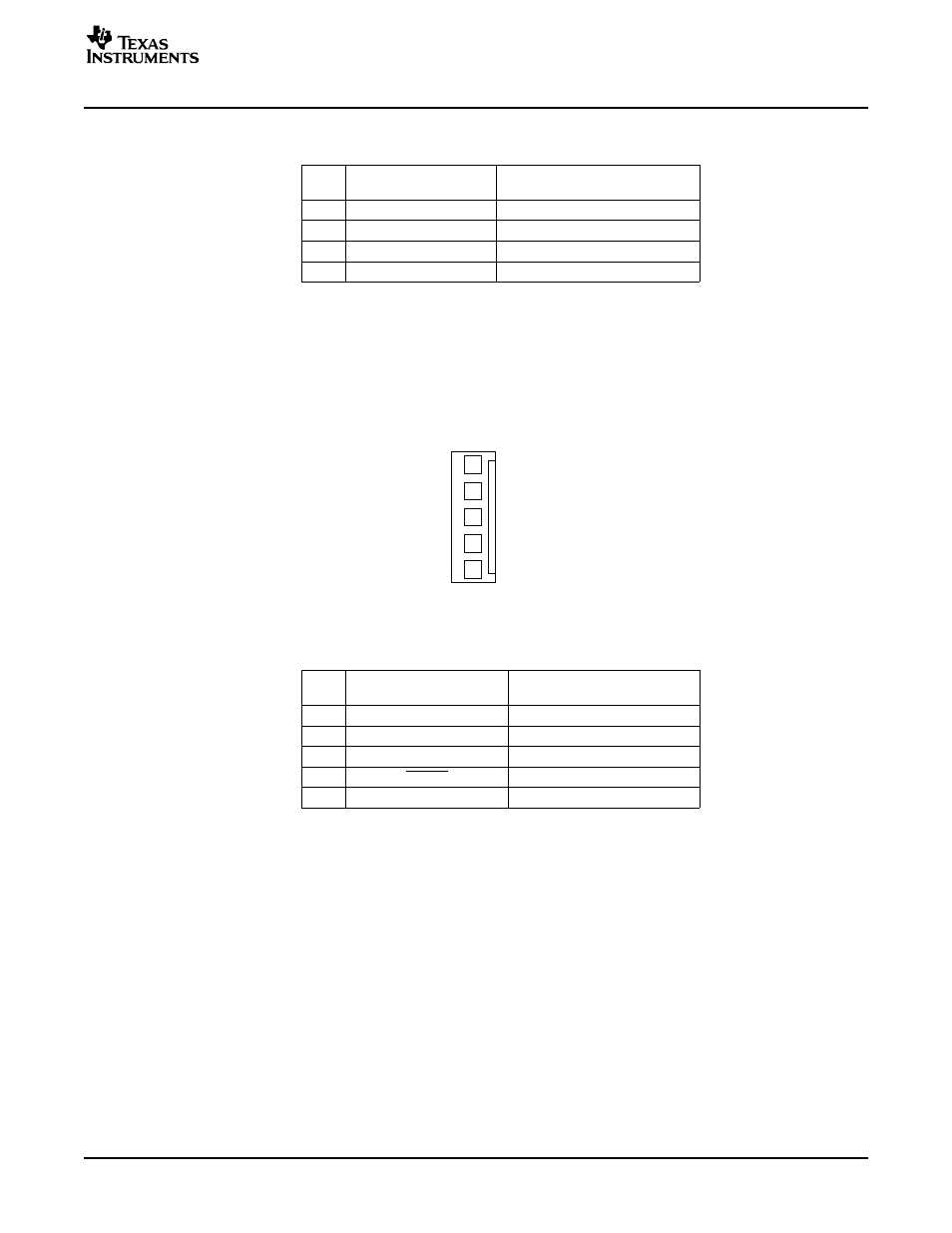
Figure 2-3. J902 Pin Numbers
Table 2-4. J902 Pin Description
PIN
NET NAME
DESCRIPTION
NO.
AT SCHEMATICS
1
–
Reserved for future use
2
PVDD
Sense of output power supply
3
GND
Ground
4
RESET
System reset (bidirectional)
5
PSVC
Power supply volume control
SLEU074 – June 2006
System Interfaces
13
See also other documents in the category Texas Instruments Receivers and Amplifiers:
- THS4151 (26 pages)
- TRF1500 (74 pages)
- SLOU082 (28 pages)
- TAS5508-5121K8EVM (24 pages)
- TPA6102A2 (16 pages)
- TPA3001D1EVM (22 pages)
- TPA6030A4 (25 pages)
- TPA701 (26 pages)
- TPA6110A2 MSOP (18 pages)
- TAS5727 (21 pages)
- THS4503EVM (28 pages)
- TPA005D02 (50 pages)
- SLOU121 (42 pages)
- TPA0243 (20 pages)
- TPA0253 (20 pages)
- TPA102 MSOP (26 pages)
- THS4131 (26 pages)
- SLOU020A (28 pages)
- TPA751 MSOP (20 pages)
- TPA005D12 (44 pages)
- TPA6139A2 EVM (8 pages)
- TPA0103 (32 pages)
- SLOU106 (26 pages)
- THS4141 (26 pages)
- THS3001 (20 pages)
- TPA0233 (20 pages)
- TPA2008D2 (26 pages)
- 2004 (20 pages)
- TPA3003D2 (36 pages)
- SLAU081 (44 pages)
- TPA301 (28 pages)
- TPA3100D2 (11 pages)
- SLOU023A (26 pages)
- TAS5110D6REF (45 pages)
- TA5704EVM (27 pages)
- APA100 (42 pages)
- TPA3200D1 (30 pages)
- TAS5066PAG (22 pages)
- TPA6204A1 (16 pages)
- THS4150 (26 pages)
- TPA311 (28 pages)
- TPA3008D2 (31 pages)
- TPA6101A2 (16 pages)