Oki MSM80C154S User Manual
Page 31
289
MSM80C154S/83C154S
¡ Semiconductor
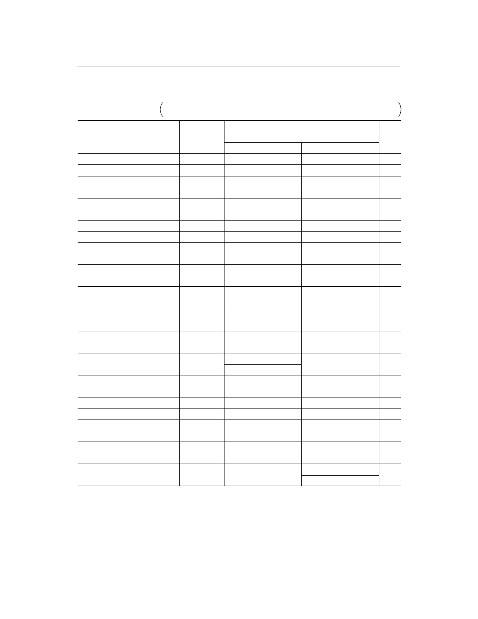
(3) External data memory access AC characteristics
*1 The variable check is from 0 to 24 MHz when the external check is used.
*2 For 2.2
£V
CC
<4 V
Parameter
Symbol
Unit
Min.
Max.
1 to 24 MHz
Variable clock from
41.7
1000
ns
t
CLCL
XTAL1, XTAL2 Oscillator Cycle
2t
CLCL
-40
—
ns
t
LHLL
ALE Signal Width
1t
CLCL
-15
—
ns
t
AVLL
Address Setup Time
(to ALE Falling Edge)
1t
CLCL
-35
—
ns
t
LLAX
Address Hold Time
(from ALE Falling Edge)
6t
CLCL
-100
—
ns
t
RLRL
RD Signal Width
6t
CLCL
-100
—
ns
t
WLWH
WR Signal Width
—
5t
CLCL
-105
ns
t
RLDV
RAM Data Read Time
(from
RD Signal Falling Edge)
0
—
ns
t
RHDX
RAM Data Read Hold Time
(from
RD Signal Rising Edge)
—
2t
CLCL
-70
ns
t
RHDZ
Data Bus Floating Time
(from
RD Signal Rising Edge)
—
8t
CLCL
-100
ns
t
LLDV
RAM Data Read Time
(from ALE Signal Falling Edge)
—
9t
CLCL
-105
ns
t
AVDV
RAM Data Read Time
(from Address Output)
3t
CLCL
-40
3t
CLCL
+40
ns
t
LLWL
RD/WR Output Time from ALE
Falling Edge
4t
CLCL
-70
—
ns
t
AVWL
RD/WR Output Time from Address
Output
1t
CLCL
-40
—
ns
t
QVWX
WR Output Time from Data Output
7t
CLCL
-105
—
ns
t
QVWH
Time from Data to
WR Rising Edge
2t
CLCL
-50
—
ns
t
WHQX
Data Hold Time
(from
WR Rising Edge)
0
—
ns
t
RLAZ
Time from to Address Float
RD
Output
1t
CLCL
-30
1t
CLCL
+40
ns
t
WHLH
Time from
RD/WR Rising Edge to
ALE Rising Edge
*1
3t
CLCL
-100
*2
*2
1t
CLCL
+100
V
CC
=2.2 to 6.0V, V
SS
=0V, Ta=–40°C to +85°C
PORT 0, ALE, and
PSEN connected with 100pF load, other connected with 80pF load