Precautions, 1 restriction for using the emulator – Renesas Converter Board R0E436049CFJ10 User Manual
Page 4
(4/6)
7. Precautions
7.1 Restriction for Using the Emulator
(1) Precautions for the register access
Please take notice the following precautions for register access because there are differences between the product chip and an
evaluation chip.
The description given in the hardware manual is “Initial value: 0. Reserved. These bits are always read as 0”. However, the
description in the evaluation chip is “Always specify 0. These bits are always read as the specify values”.
Target address and bit:
Bits 7, 6 and 5 of address H’FFFFE2 (Port mode register 3)
Bits 7 and 6 of address H’FFFFF5 (Interrupt enable register 2)
Bit
7
of
address
H’FFFFF9 (Module standby control register 1)
Bits 6, 5 and 3 of address H’FFFFFA (Module standby control register 2)
The description in the hardware manual is “Reserved”. However, the description in the evaluation chip is “Always specify 0. These
bits are always read as the specified values”.
Target address and bit:
Bit 0 of address H’FFFFFB
The hardware manual shows registers at the addresses given below. For these locations, however, the applicable description in the
evaluation chip is “Writing has no effect. These bits are always read as undefined values”, because there are no registers at these
locations of the evaluation chip.
Target address:
H’FFF730 (Low-voltage-detection control register)
H’FFF731
(Low-voltage-detection status register)
H’FFFF90 (Flash memory control register 1)
H’FFFF91 (Flash memory control register 2)
H’FFFF92 (Flash memory power control register)
H’FFFF93
(Erase
block
register
1)
H’FFFF9B (Flash memory enable register)
(2) Note on Power-on Reset and Low-voltage Detection Circuit Functions
The product chip has optional functions of power-on reset and low-voltage detection circuit and can select them. However, since
the evaluation chip does not support these functions, software debugging cannot be performed in the emulator. Be sure to
evaluate your system and make final confirmation with a product chip.
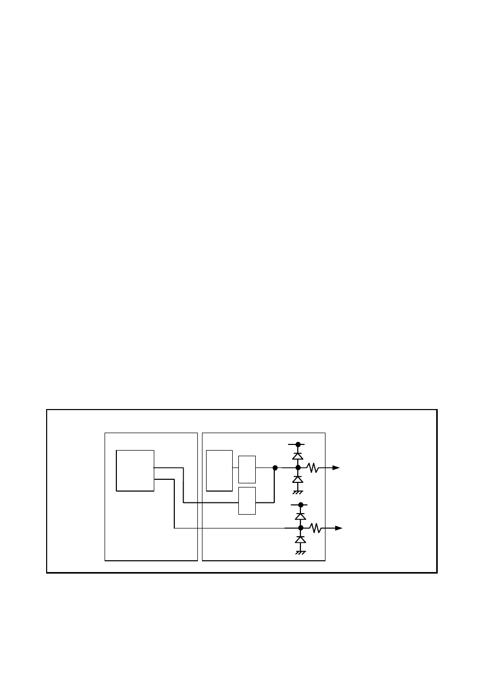
(3) Note on Serial Interface SCI3_3
Because the evaluation chip does not incorporate the SCI3_3 module, it emulates the SCI3_3 function by connecting an external
circuit on the R0E436049CFJ10. When using the SCI3_3, be sure to set the multiplexed port control registers (PCR: P90, P91
and P92) to “0” (input) beforehand. If using emulators, set the bit 3 of the address H’FFF608 (Serial mode control register3) to
“1”.
EVACHIP
R0E436640CPE00
R0E436049CFJ10
User
System
FPGA
Level
converver
22Ω
47Ω
Analog SW
P90,P91,P92
Others
P12,P56,P57
Figure 5 Connections of the R0E436049CFJ10