Hardware configuration of the m30262t-ptc, Connection procedure, Switch settings – Renesas M30262T-PTC User Manual
Page 3: Connection procedure (see figure 4), When you use no. 36 pin (port p1, Ma de in ja pa n

( 3/4 )
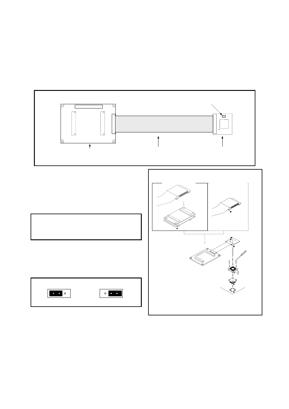
5. Hardware Configuration of the M30262T-PTC (See Figure 3)
Hardware configuration of the M30262T-PTC is shown below.
(1) Connector
Connector for the emulator for M16C/62P (M3062PT-EPB).
(2) Cable
Flat cable which connects the user system flexibly (Length: 150 mm).
(3) Target
interface
Interface which has a connector for a user system and jumper switch JP1.
Figure 3 Hardware configuration of the M30262T-PTC
6. Connection Procedure (see Figure 4)
The procedure for connecting the M30262T-PTC is shown below.
(1) Mount the NQPACK048SD.
(2) Mount the YQPACK048SD on the NQPACK048SD.
(3) Secure the four corners of the YQPACK048SD with
the YQ-GUIDE's.
Do NOT use the screws in the YQPACK048SD package.
Do NOT use the screwdriver in the NQPACK048SD
package for securing YQ-GUIDE's (used for securing
HQPACK048SD).
(4) Attach the M30262T-PTC to the YQPACK048SD.
(5) Connect the emulator for M16C/62P to the M30262T-PTC.
7. Switch Settings
When you use No. 36 pin (Port P1
5
/INT
3
/ADTRG),
set switch JP1 according to port functions.
Figure 5 JP1 Settings
Figure 4 Connection Procedure
YQ-GUIDE’s
(x4)
YQPACK048SD
NQPACK048SD
48-pin 0.5-mm-pitch
(48P6Q-A) foot pattern
(1)
(2)
(3)
(5)
(4)
Use a flat-blade
screwdriver.
M30262T-PTCB
M3
02
62
T-
PT
CB
R
EV
.A
M1
6C
/62
P
TO
OL
SI
D
E
M3
02
62
T-
PT
C
RE
V.A
MA
DE
IN
JA
PA
N
MA
DE
IN
JA
PA
N
PC7501
M3062PT-EPB
Emulator for 16C/62P
( PC7501 + M3062PT-EPB )
( PC4701 + M3062PT3-RPD-E )
M3062PT3-RPD-E
40b
1b
40a
1a
40b
1b
40a
1a
1
50
J1
J2
CN1
M30262T-PTCB REV.A
M16C/62P TOOL SIDE
JP1
IC1
1
M30262T-PTC REV.A
1
50
P
15/
IN
T
3
AD
T
R
G
Connector
Cable (FFC cable : 150 mm)
Target interface
Jumper switch JP1
For ADTRG
For P15 or INT3
ADT
R
G
P15
/IN
T
3
JP1
AD
TR
G
P15
/IN
T3
JP1
