Renesas H8SX/1668R User Manual
Page 18
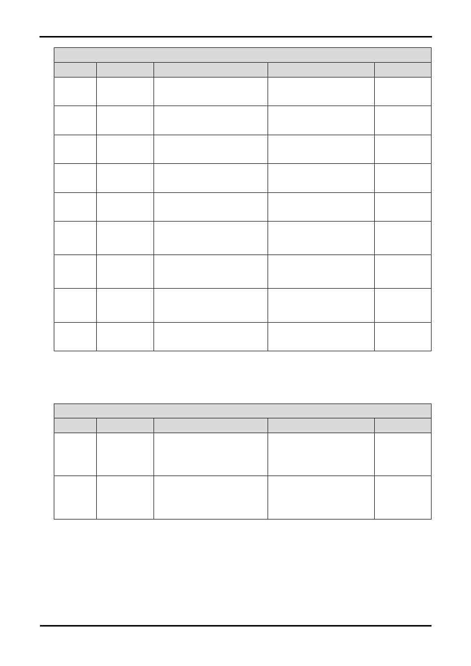
Option Link Settings
Reference
Function
Fitted
Alternative (Removed)
Related To
R93 32.768
KHz
Clock Oscillator
Routes OSC1 CPU pin to J3 header OSC1 CPU pin and J3 header
are not connected
R94, R103,
R105
R94 32.768
KHz
Clock Oscillator
Routes OSC2 CPU pin to J3 header OSC2 CPU pin and J3 header
are not connected
R93, R103,
R105
R103 32.768
KHz
Clock Oscillator
On-board low-speed clock source
is used
External clock source is used
R93, R94, R104
R105 32.768
KHz
Clock Oscillator
On-board low-speed clock source
is used
External clock source is used
R94, R93, R103
R98 32.768
KHz
Clock Oscillator
Parallel resistor for a crystal
Not fitted
-
R99
12 MHz Clock
Oscillator
Routes EXTAL CPU pin to J3
header.
EXTAL CPU pin and J3 header
are not connected
R102, R101,
R100
R102
12 MHz Clock
Oscillator
Routes XTAL CPU pin to J3 and JA2
headers
XTAL CPU pin and J3 and JA2
headers are not connected
R99, R101,
R100
R101
12 MHz Clock
Oscillator
On-board main clock source is
used
External clock source is used
R99, R102
R100
12 MHz Clock
Oscillator
Parallel resistor for a crystal
Not fitted
-
Table 6-9: Clock configuration links.
Table 6-10 below describes the function of the option links associated with reference voltage source. The default configuration is indicated
by BOLD text.
Option Link Settings
Reference
Function
Fitted
Alternative (Removed)
Related To
R64 Voltage
Reference
Source
Voltage Reference set to
Board_ Vcc signal.
Voltage Reference taken from
external connector.
R83
R83 Voltage
Reference
Source
Voltage Reference is taken from
external connector.
Voltage Reference set to
Board_Vcc signal.
R64
Table 6-10: Voltage reference links.
Table 6-11 below describes the function of the option links associated with analog power supply. The default configuration is indicated by
BOLD text.
16