Switching characteristics, Parameter measurement information – National DS36C278 User Manual
Page 4
Switching Characteristics
(Continued)
Over Supply Voltage and Operating Temperature ranges unless otherwise specified (Notes 3 and 8)
Symbol
Parameter
Conditions
Reference
Min
Typ
Max
Units
RECEIVER CHARACTERISTICS
t
PHL
Propagation Delay
C
L
e
15 pF
Figures 12 13
30
210
400
ns
High to Low
t
PLH
Propagation Delay
30
190
400
ns
Low to High
t
SK
Skew
l
t
PHL
b
t
PLH
l
0
20
50
ns
t
PLZ
Output Disable Time
C
L
e
15 pF
Figures 14 15 16
50
150
ns
t
PHZ
55
150
ns
t
PZL
Output Enable Time
40
150
ns
t
PZH
45
150
ns
Note 1
‘‘Absolute Maximum Ratings’’ are those values beyond which the safety of the device cannot be guaranteed They are not meant to imply that the devices
should be operated at these limits The table of ‘‘Electrical Characteristics’’ specifies conditions of device operation
Note 2
Current into device pins is defined as positive Current out of device pins is defined as negative All voltages are referenced to ground except V
OD1
and
V
OD2
Note 3
All typicals are given for V
CC
e a
5 0V T
A
e a
25 C
Note 4
Delta
l
V
OD2
l
and Delta
l
V
OC
l
are changes in magnitude of V
OD2
and V
OC
respectively that occur when input changes state
Note 5
Threshold parameter limits specified as an algebraic value rather than by magnitude
Note 6
Hysteresis defined as V
HST
e
V
TH
b
V
TL
Note 7
I
IN
includes the receiver input current and driver TRI-STATE leakage current
Note 8
C
L
includes probe and jig capacitance
Note 9
For complete details of test see RS-485
Parameter Measurement Information
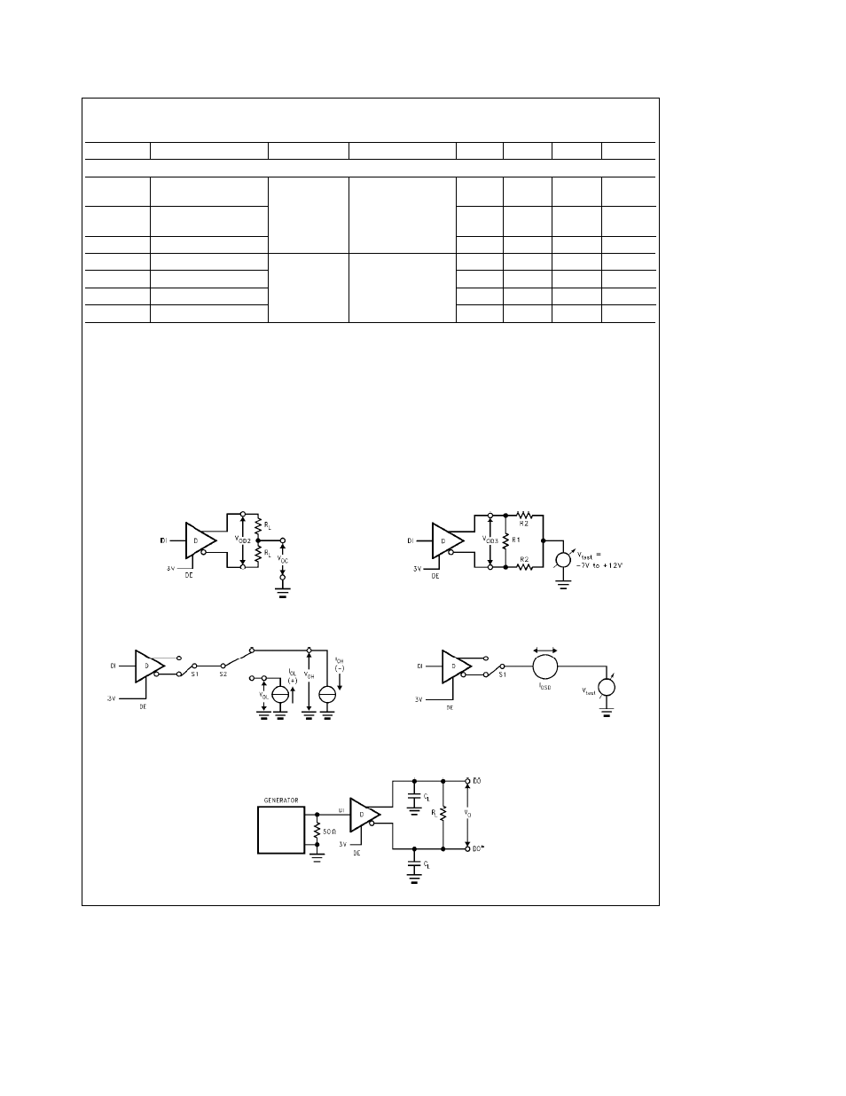
TL F 12040 – 2
FIGURE 1 Driver V
OD2
and V
OC
TL F 12040 – 18
FIGURE 2 Driver V
OD3
TL F 12040 – 3
FIGURE 3 Driver V
OH
and V
OL
TL F 12040 – 4
Vtest e b7V to a12V
FIGURE 4 Driver I
OSD
TL F 12040 – 5
FIGURE 5 Driver Differential Propagation Delay Test Circuit
http
www national com
4