Absolute maximum ratings, Recommended operating conditions, Electrical characteristics – National DS36C278 User Manual
Page 2
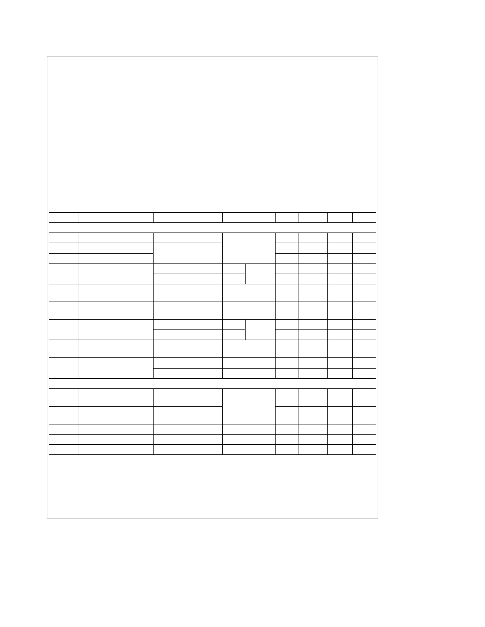
Absolute Maximum Ratings
(Note 1)
If Military Aerospace specified devices are required
please contact the National Semiconductor Sales
Office Distributors for availability and specifications
Supply Voltage (V
CC
)
a
12V
Input Voltage (DE RE
DI)
b
0 5V to (V
CC
a
0 5V)
Common Mode (V
CM
)
Driver Output Receiver Input
g
15V
Input Voltage (DO RI DO
RI )
g
14V
Receiver Output Voltage
b
0 5V to (V
CC
a
0 5V)
Maximum Package Power Dissipation
a
25 C
M Package 1190 mW derate
9 5 mW C above a25 C
N Package 744 mW derate
6 0 mW C above a25 C
Storage Temperature Range
b
65 C to a150 C
Lead Temperature (Soldering 4 sec)
a
260 C
Recommended Operating
Conditions
Min
Typ
Max
Units
Supply Voltage (V
CC
)
a
4 75
a
5 0
a
5 25
V
Bus Voltage
b
7
a
12
V
Operating Free Air Temperature (Ta)
DS36C278T
b
40
25
a
85
C
DS36C278
0
25
a
70
C
Electrical Characteristics
Over Supply Voltage and Operating Temperature ranges unless otherwise specified (Notes 2 and 3)
Symbol
Parameter
Conditions
Reference
Min
Typ
Max
Units
DIFFERENTIAL DRIVER CHARACTERISTICS
V
OD1
Differential Output Voltage
I
O
e
0 mA (No Load)
(485)
(422)
1 5
5 0
V
V
OD0
Output Voltage
I
O
e
0 mA
0
5 0
V
V
OD0
Output Voltage
(Output to GND)
0
5 0
V
V
OD2
Differential Output Voltage
R
L
e
50X
(422)
Figure 1
2 0
2 8
V
(Termination Load)
R
L
e
27X
(485)
1 5
2 3
5 0
V
D
V
OD2
Balance of V
OD2
R
L
e
27X or 50X
(Note 4)
b
0 2
0 1
a
0 2
V
l
V
OD2
b
V
OD2
l
(422 485)
V
OD3
Differential Output Voltage
R1 e 54X R2 e 375X
Figure 2
1 5
2 0
5 0
V
(Full Load)
V
TEST
e b
7V to a12V
V
OC
Driver Common Mode
R
L
e
27X
(485)
Figure 1
0
3 0
V
Output Voltage
R
L
e
50X
(422)
0
3 0
V
D
V
OC
Balance of V
OC
R
L
e
27X or
(Note 4)
b
0 2
a
0 2
V
l
V
OC
b
V
OC
l
R
L
e
50X
(422 485)
I
OSD
Driver Output Short-Circuit
V
O
e a
12V
(485)
Figure 4
200
a
250
mA
Current
V
O
e b
7V
(485)
b
190
b
250
mA
RECEIVER CHARACTERISTICS
V
TH
Differential Input High
V
O
e
V
OH
I
O
e b
0 4V
(422 485)
(Note 5)
a
0 035
a
0 2
V
Threshold Voltage
b
7V
s
V
CM
s
a
12V
V
TL
Differential Input Low
V
O
e
V
OL
I
O
e
0 4 mA
b
0 2
b
0 035
V
Threshold Voltage
b
7V
s
V
CM
s
a
12V
V
HST
Hysteresis
V
CM
e
0V
(Note 6)
70
mV
R
IN
Input Resistance
b
7V
s
V
CM
s
a
12V
DS36C278T
24
68
kX
R
IN
Input Resistance
b
7V
s
V
CM
s
a
12V
DS36C278
48
68
kX
http
www national com
2