Limiting values, Thermal resistance, Characteristics – Philips BGA2711 User Manual
Page 3: Mmic wideband amplifier bga2711
2001 Oct 19
3
NXP Semiconductors
Product specification
MMIC wideband amplifier
BGA2711
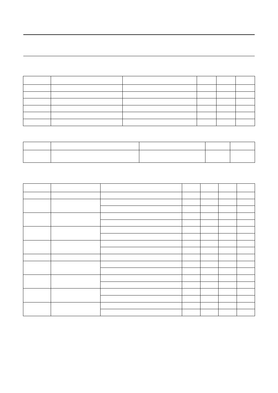
LIMITING VALUES
In accordance with the Absolute Maximum Rating System (IEC 60134)
THERMAL RESISTANCE
CHARACTERISTICS
V
S
= 5 V; I
S
= 12.6 mA; f = 1 GHz; T
j
= 25
C unless otherwise specified.
SYMBOL
PARAMETER
CONDITIONS
MIN.
MAX.
UNIT
V
S
DC supply voltage
RF input AC coupled
6
V
I
S
supply current
20
mA
P
tot
total power dissipation
T
s
80 C
200
mW
T
stg
storage temperature
65
+150
C
T
j
operating junction temperature
150
C
P
D
maximum drive power
10
dBm
SYMBOL
PARAMETER
CONDITIONS
VALUE
UNIT
R
th j-s
thermal resistance from junction to solder
point
P
tot
= 200 mW; T
s
80 C
300
K/W
SYMBOL
PARAMETER
CONDITIONS
MIN.
TYP.
MAX.
UNIT
I
S
supply current
10
12.6
16
mA
|s
21
|
2
insertion power gain
f = 1 GHz
13.1
dB
f = 2 GHz
13.9
dB
R
L
IN
return losses input
f = 1 GHz
11
dB
f = 2 GHz
10
dB
R
L
OUT
return losses output
f = 1 GHz
18
dB
f = 2 GHz
13
dB
NF
noise figure
f = 1 GHz
4.8
dB
f = 2 GHz
4.8
dB
BW
bandwidth
at
s
21
2
3 dB below flat gain at 1 GHz
3.6
GHz
P
L(sat)
saturated load power
f = 1 GHz
2.8
dBm
f = 2 GHz
0.6
dBm
P
L 1 dB
load power
at 1 dB gain compression; f = 1 GHz
0.7
dBm
at 1 dB gain compression; f = 2 GHz
1.8
dBm
IP3
(in)
input intercept point
f = 1 GHz
4.8
dBm
f = 2 GHz
8.5
dBm
IP3
(out)
output intercept point
f = 1 GHz
8.3
dBm
f = 2 GHz
5.4
dBm