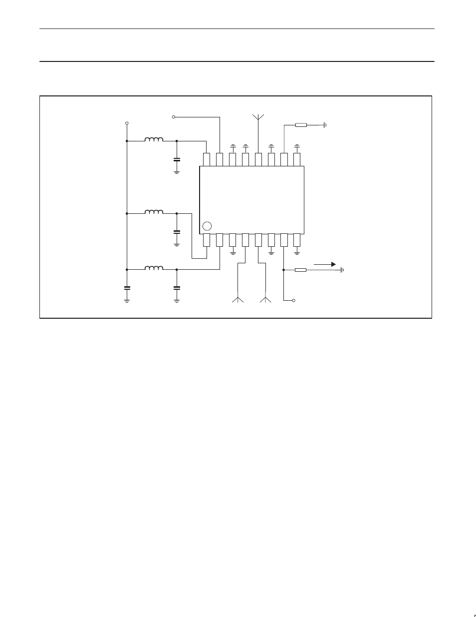
Connectivity diagram – Philips SA2411 User Manual
Page 5

Philips Semiconductors
Product data
SA2411
+20 dBm single chip linear amplifier for WLAN
2003 Feb 07
5
7. CONNECTIVITY DIAGRAM
SR02385
C2
C1
C4
C3
L3
L2
PWRUP
RFin
ANT
L1
VDD
VDD
GND
IN+
IN–
GND
DET
GND
VDD
PwrUp
GND
GND
ANT
GND
MODE
GND
RFin
R1
R2
Idet.
V
det
V
DD
SA2411
C1, C2, C3
= 5.6 pF
C4
= 10 nF
R1
= optional connect to ground via 0
W
resistor.
R2
= optional resistor to ground to convert current into voltage
L1, L2, L3
= Optional inductors
1 nH
…
10 nH, or microstrip lines with length 1
…
10 mm.
No inductors and directly connecting all supplies to V
DD
might cause problems. The optimal values of the inductors
depends on the application board.
See also other documents in the category Philips Receivers and Amplifiers:
- SA58605 (9 pages)
- TDA1596T (22 pages)
- UA741C (7 pages)
- BGX885N (8 pages)
- TDA8946J (23 pages)
- BGY280 (11 pages)
- SWS2083W/17 (2 pages)
- MC1558 (6 pages)
- BGY148B (12 pages)
- HTR5205 (3 pages)
- TDA8559T (36 pages)
- TDA8542 (20 pages)
- TDA7056A (9 pages)
- TDA1552Q (10 pages)
- TDA7052A (12 pages)
- Audio/Video Selector US2-PH61150 (2 pages)
- SA5512 (4 pages)
- TDA8943SF (12 pages)
- SWV2064 (2 pages)
- BGY583 (8 pages)
- SWS2326W (2 pages)
- DTR 7510 (60 pages)
- HTR3464 (2 pages)
- BGD885 (8 pages)
- SA5205A (13 pages)
- CGY2014TT (16 pages)
- SWV2116 (2 pages)
- TDA6111Q (16 pages)
- SWS2063W (2 pages)
- TFA9843AJ (19 pages)
- BGA6489 (13 pages)
- BGY86 (8 pages)
- BGM1012 (13 pages)
- HTS8000S (49 pages)
- TDA7053A (16 pages)
- FR-975 (92 pages)
- TDA1015 (13 pages)
- SA5211 (28 pages)
- TDA6107AJF (16 pages)
- BGY883 (7 pages)
- TDA7050 (8 pages)
- SWV2063 (2 pages)
- BGY885B (8 pages)
- 14RF50S (2 pages)
- 14RF50S (44 pages)
