Philips UA733 User Manual
Page 3
Philips Semiconductors Linear Products
Product specification
µ
A733/733C
Differential video amplifier
April 15, 1992
264
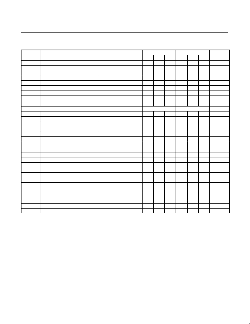
DC ELECTRICAL CHARACTERISTICS
(Continued)
SYMBOL
PARAMETER
TEST CONDITIONS
µ
A733C
µ
A733
UNIT
SYMBOL
PARAMETER
TEST CONDITIONS
Min
Typ
Max
Min
Typ
Max
UNIT
SVRR
Supply voltage rejection ratio Gain 2
∆
V
S
=
±
0.5V
50
70
50
70
dB
Output offset voltage
R
L
=
∞
Gain 1
1
0.6
1.5
0.6
1.5
V
Gain 2 and 3
2, 3
0.35
1.5
0.35
1.0
V
V
CM
Output common-mode voltage
R
L
=
∞
2.4
2.9
3.4
2.4
2.9
3.4
V
Output voltage swing, differential
R
L
=2k
Ω
3.0
4.0
3.0
4.0
V
P-P
I
SINK
Output sink current
2.5
3.6
2.5
3.6
mA
R
OUT
Output resistance
20
20
Ω
I
CC
Power supply current
R
L
=
∞
18
24
18
24
mA
THE FOLLOWING SPECIFICATIONS APPLY OVER TEMPERATURE
0
°
C
≤
T
A
≤
70
°
C
-55
°
C
≤
T
A
≤
125
°
C
Min
Typ
Max
Min
Typ
Max
UNIT
Differential voltage gain
R
I
= 2k
Ω
, V
OUT
= 3V
P-P
Gain 1
1
250
600
200
600
V/V
Gain 2
2
80
120
80
120
V/V
Gain
3
8
12
8
12
V/V
R
IN
Input resistance
Gain 2
2
8
8
k
Ω
I
OS
Input offset current
6
5
µ
A
I
BIAS
Input bias current
40
40
µ
A
V
IN
Input voltage range
±
1.0
±
1.0
V
CMRR
Common-mode rejection ratio
Gain 2
V
CM
=
±
V, F
≤
100kHz
50
50
dB
SVRR
Supply voltage rejection ratio
Gain 2
∆
V
S
=
±
0.5V
50
50
dB
V
OS
Output offset voltage
R
L
=
∞
Gain 1
1
1.5
1.5
V
Gain 2 and 3
2, 3
1.5
1.2
V
V
DIFF
Output voltage swing, differential
R
L
= 2k
Ω
2.8
2.5
V
P-P
I
SINK
Output sink current
2.5
2.2
mA
I
CC
Power supply current
R
L
± ∞
27
27
mA
NOTES:
1. Gain select pins G
1A
and G
1B
connected together.
2. Gain select pins G
2A
and G
2B
connected together.
3. All gain select pins open.