Mds-nt1 – Sony MDS-NT1 User Manual
Page 57
57
MDS-NT1
•
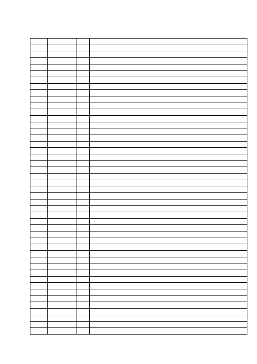
MAIN BOARD IC301 CXD1873R (NET MD SECURITY, DIGITAL SIGNAL PROCESSOR, USB INTERFACE)
Pin No.
Pin Name
I/O
Description
1
VDEA0
—
Power supply terminal (+3.3V) (for DSP)
2
VSEA0
—
Ground terminal (for DSP)
3
PLLSW
I
PLL function on/off control signal input from the system controller “L”: PLL on
4
TEST0
I
Test input terminal Normally fixed at “L”
5
DSPCLK
I
DSP transfer clock signal input terminal (256Fs: 11.2896MHz)
6
VDC0
—
Power supply terminal (+3.3V)
7
DSPIF0
O
Digital audio signal output terminal when recording mode
8
DSPIF1
O
L/R sampling clock signal (44.1 kHz) output terminal
9
VDEA1
—
Power supply terminal (+3.3V) (for DSP)
10
DSPIF2
O
Bit clock signal (2.8224 MHz) output terminal
11
DSPIF3
O
Recording data output terminal
12
VDC1
—
Power supply terminal (+3.3V)
13
VSC0
—
Ground terminal
14
EXTIF0
I/O
Not used
15
EXTIF1
I/O
Not used
16
VDEA2
—
Power supply terminal (+3.3V) (for DSP)
17
VSEA1
—
Ground terminal (for DSP)
18
EXTIF0
I/O
Not used
19
EXTIF1
I/O
Not used
20
VDC2
—
Power supply terminal (+3.3V)
21
VSC1
—
Ground terminal
22
DNKCK
O
Serial ROM clock signal output terminal Not used
23
DNKCS
O
Serial ROM chip select signal output terminal Not used
24
VDEA3
—
Power supply terminal (+3.3V) (for DSP)
25
VSEA2
—
Ground terminal (for DSP)
26
DNKSO
O
Serial ROM data output terminal Not used
27
DNKSI
I
Serial ROM data input terminal Not used
28
DNKST
I
Serial ROM status input terminal Not used
29
VDC3
—
Power supply terminal (+3.3V)
30
VSC2
—
Ground terminal
31
DNKRS
I
Serial ROM reset signal input terminal Not used
32
TEST1
I
Test input terminal Normally fixed at “L”
33
VDEA4
—
Power supply terminal (+3.3V) (for DSP)
34
PLLTHRU
I
Not used
35
USBEN
I
USB enable signal input terminal
36
VDC4
—
Power supply terminal (+3.3V)
37
VSC3
—
Ground terminal
38
USBVSS
—
Ground terminal (for USB)
39
DP
I/O
USB communication input/output
40
DM
I/O
USB communication input/output
41
USBVDD
—
Power supply terminal (+3.3V) (for USB)
42
USBSW
O
USB communication on/off control signal output “H”: USB communication on
43
PLLVDD
—
Power supply terminal (+3.3V) (for USB)
44
PLLVSS
—
Ground terminal (for USB)
45
OSCVDD
—
Power supply terminal (+3.3V) (for OSC)