Target board, Led headers (j1, j2, j3, j4), Table 1. j2 and j3 led locations – Silicon Laboratories CP2112-EK User Manual
Page 6: C p 2 11 2 - e k
C P 2 11 2 - E K
6
Rev. 0.2
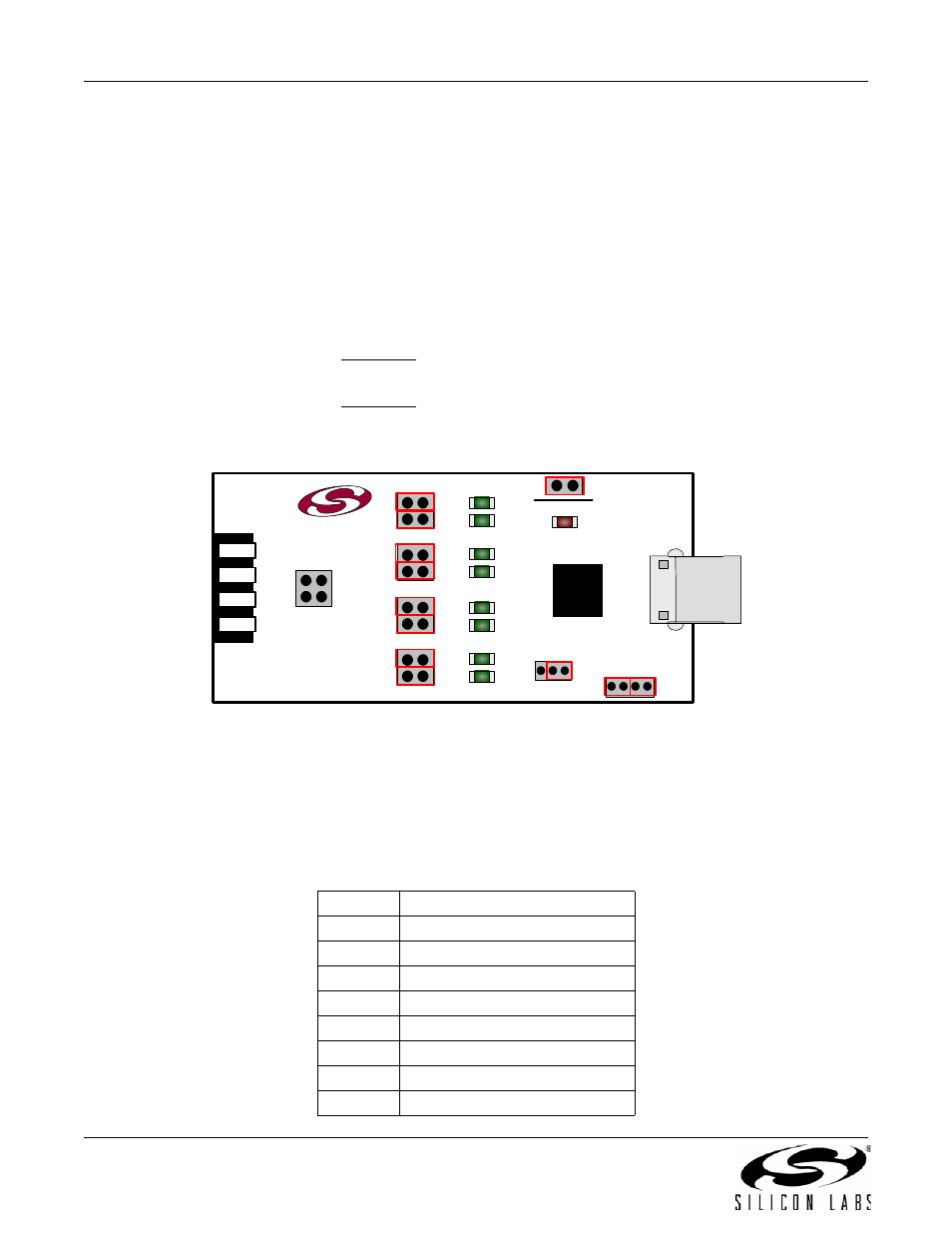
5. Target Board
The CP2112 Evaluation Kit includes an evaluation board with a CP2112 device pre-installed for evaluation and
preliminary software development. Numerous input/output (I/O) connections are provided to facilitate prototyping
using the evaluation board. Refer to Figure 6 for the locations of the various I/O connectors. Refer to Figure 7,
“CP2112 Evaluation Board Schematic” for information regarding the SMBus pull-up resistors that are located on
the target board.
P1
USB connector for USB interface
H1
Access Connector for SMBus interface (SDA, SCL, GND, Pull-Up Voltage)
J1, J2, J3, J4
GPIO access connectors
J6
Power connector
J7
SMBus pull-up voltage connector
J8
Red SUSPEND LED connector
DS0–DS7
Green GPIO LEDs
DS8
Red SUSPEND LED
TB1
SMBus interface terminal block
Figure 6. CP2112 Evaluation Board with Default Shorting Blocks Installed
5.1. LED Headers (J1, J2, J3, J4)
Connectors J1, J2, J3, and J4 are provided to allow access to the GPIO pins on the CP2112. Place shorting blocks
on J1, J2, J3, and J4 to connect the GPIO pins to the eight green LEDs, DS0–DS7. These LEDs can be used to
indicate active communications through the CP2112. Table 1 lists the LED corresponding to each header position.
Table 1. J2 and J3 LED Locations
LED
Pins
DS0
J1[3:4]
DS1
J1[1:2]
DS2
J2[3:4]
DS3
J2[1:2]
DS4
J3[3:4]
DS5
J3[1:2]
DS6
J4[3:4]
DS7
J4[1:2]
GND
SDA
SCL
EXT_PU
H1
GND
EXT_PU
J4
J3
J2
J1
DS7
DS6
DS5
DS4
DS3
DS2
DS1
DS0
CP2112
U1
SILICON LABS
www.silabs.com
P1
CP2112-EK
J7
J6
SMBUS PU_V
EX
T
_
PU
VI
O
VI
O
VD
D
+3V NE
T
A
TB1
DS8
SUSPEND
J8