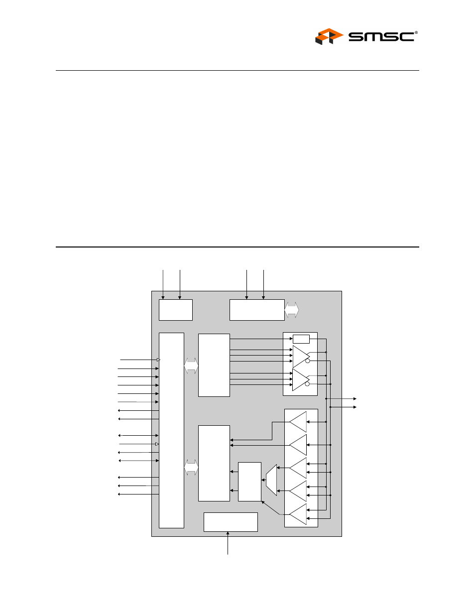
General description, Block diagram, Figure 1 usb3250 functional block diagram – SMSC USB3250 User Manual
Page 3: Product preview

Hi-Speed USB Device Transceiver with UTMI Interface
SMSC USB3250
3
Revision 1.7 (05-11-07)
PRODUCT PREVIEW
General Description
The USB3250 provides the Physical Layer (PHY) interface to a USB 2.0 Device Controller. The IC is
available in a 56 pin QFN.
The USB3250 is a USB 2.0 physical layer transceiver (PHY) integrated circuit. SMSC's proprietary
technology results in low power dissipation, which is ideal for building a bus powered USB 2.0
peripheral. The PHY can be configured for either an 8-bit unidirectional or a 16-bit bidirectional parallel
interface, which complies with the USB Transceiver Macrocell Interface (UTMI) specification. It
supports 480Mbps transfer rate, while remaining backward compatible with USB 1.1 legacy protocol
at 12Mbps.
All required termination for the USB 2.0 Transceiver is internal. Internal 5.25V short circuit protection
of DP and DM lines is provided for USB compliance.
While transmitting data, the PHY serializes data and generates SYNC and EOP fields. It also performs
needed bit stuffing and NRZI encoding. Likewise, while receiving data, the PHY de-serializes incoming
data, stripping SYNC and EOP fields and performs bit un-stuffing and NRZI decoding.
Block Diagram
Figure 1 USB3250 Functional Block Diagram
VALIDH
PWR
CONTROL
FS
SE+
RX
UT
MI In
terfa
ce
TX State
Machine
Parallel to
Serial
Conversion
Bit Stuff
NRZ
Encode
TX
LOGIC
Clock
Recovery Unit
Clock
and
Data
Recovery
Elasticity
Buffer
VP
VM
BIASING
Bandgap Voltage Reference
Current Reference
RB
IA
S
VD
D
3
.3
VD
D
1
.8
PLL and
XTAL OSC
System
Clocking
FS
RX
FS
SE-
HS
RX
HS
SQ
RX State
Machine
Serial to
Parallel
Conversion
Bit Unstuff
NRZI
Decode
RX
LOGIC
DM
TX
1.5kΩ
FS
TX
HS
TX
HS_DATA
HS_CS_ENABLE
HS_DRIVE_ENABLE
OEB
VMO
VPO
RPU_EN
MUX
DP
RXVALID
RXACTIVE
RXERROR
TXREADY
RESET
SUSPENDN
XCVRSELECT
TERMSELECT
OPMODE[1:0]
LINESTATE[1:0]
CLKOUT
TXVALID
DATABUS16_8
DATA[15:0] *
XI
XO
