Dual, 65msps, 12-bit, if/baseband adc, Detailed description, Pin description (continued) – Maxim Integrated MAX12527 User Manual
Page 14
MAX12527
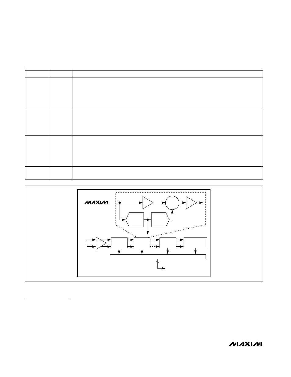
Detailed Description
The MAX12527 uses a 10-stage, fully differential,
pipelined architecture (Figure 1) that allows for high-
speed conversion while minimizing power consump-
tion. Samples taken at the inputs move progressively
through the pipeline stages every half clock cycle.
From input to output the total latency is 8 clock cycles.
Each pipeline converter stage converts its input voltage
to a digital output code. At every stage, except the last,
the error between the input voltage and the digital out-
put code is multiplied and passed along to the next
pipeline stage. Digital error correction compensates for
ADC comparator offsets in each pipeline stage and
ensures no missing codes. Figure 2 shows the
MAX12527 functional diagram.
Dual, 65Msps, 12-Bit, IF/Baseband ADC
14
______________________________________________________________________________________
PIN
NAME
FUNCTION
66
SHREF
Shared Reference Digital Input.
SHREF = V
DD
: Shared reference enabled.
SHREF = GND: Shared reference disabled.
When sharing the reference, externally connect REFAP and REFBP together to ensure that V
REFAP
equals V
REFBP
. Similarly, when sharing the reference, externally connect REFAN to REFBN together to
ensure that V
REFAN
= V
REFBN
.
67
REFOUT
Internal Reference Voltage Output. The REFOUT output voltage is 2.048V and REFOUT can deliver 1mA.
For internal reference operation, connect REFOUT directly to REFIN or use a resistive divider from
REFOUT to set the voltage at REFIN. Bypass REFOUT to GND with a
≥0.1µF capacitor.
For external reference operation, REFOUT is not required and must be bypassed to GND with a
≥0.1µF
capacitor.
68
REFIN
Single-Ended Reference Analog Input.
For internal reference and buffered external reference operation, apply a 0.7V to 2.3V DC reference
voltage to REFIN. Bypass REFIN to GND with a 4.7µF capacitor. Within its specified operating voltage,
REFIN has a >50M
Ω input impedance, and the differential reference voltage (V
REF_P
- V
REF_N
) is
generated from REFIN. For unbuffered external reference operation, connect REFIN to GND. In this
mode REF_P, REF_N, and COM_ are high-impedance inputs that accept the external reference voltages.
—
EP
Exposed Paddle. EP is internally connected to GND. Externally connect EP to GND to achieve specified
dynamic performance.
Pin Description (continued)
MAX12527
Σ
+
−
DIGITAL ERROR CORRECTION
FLASH
ADC
x2
DAC
STAGE 2
IN_P
IN_N
STAGE 1
STAGE 9
STAGE 10
END OF PIPELINE
D0_ THROUGH D11_
Figure 1. Pipeline Architecture—Stage Blocks