Bus_port, Bdm-in – Motorola MCU 68HC912D60 User Manual
Page 15
15
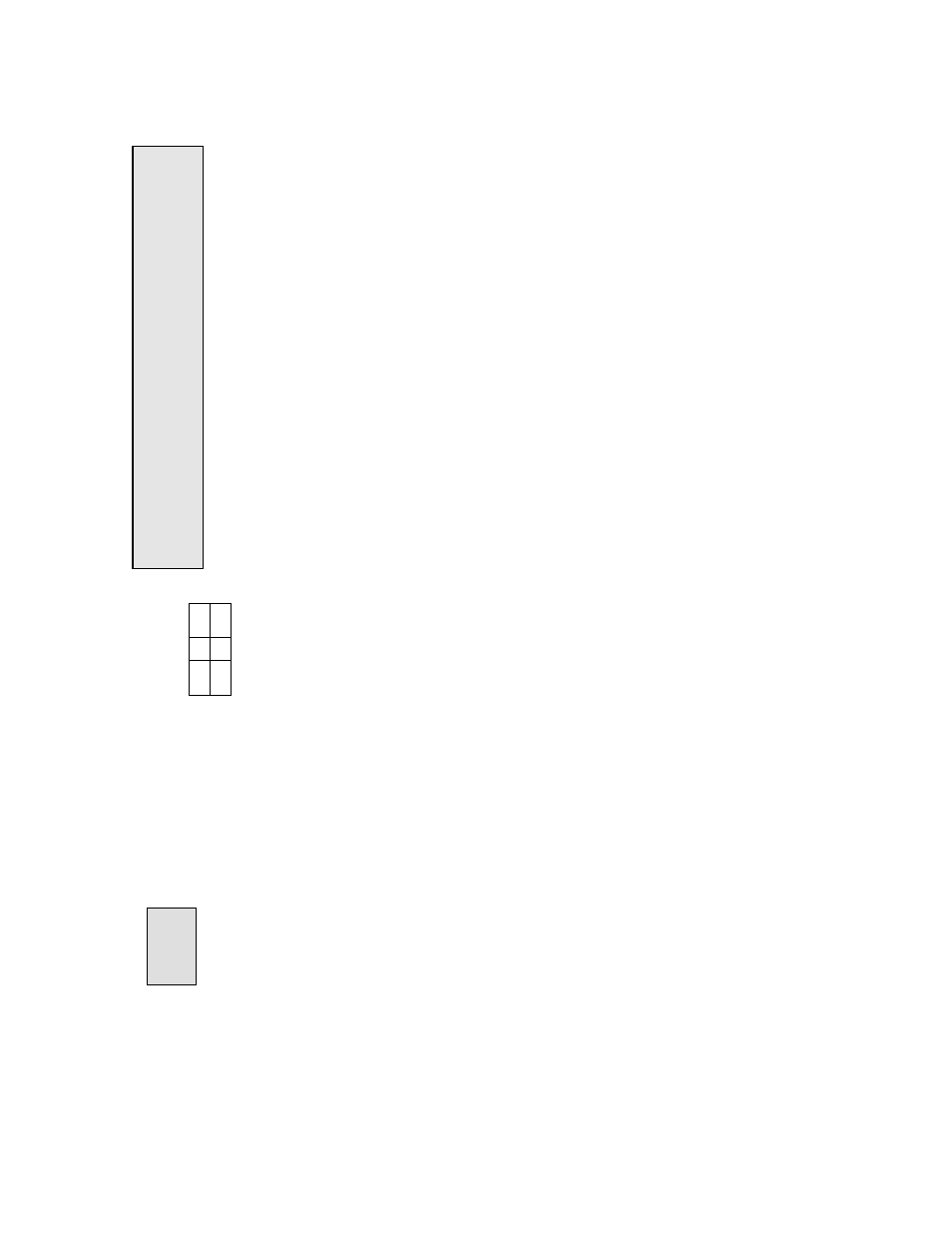
BUS_PORT
The BUS_PORT supports off-board memory devices as follows:
GND
1 2
D11
D10
3 4
D12
D9
5 6
D13
D8
7 8
D14
A0
9 10 D15
A1 11 12 A2
A10 13 14 A3
/ OE 15 16 A4
A11 17 18 A5
A9 19 20 A6
A8 21 22 A7
A12 23 24 A13
/ WE
25 26 CS0
CS1 27 28 CS2
CS3 29 30 CS4
CS5 31 32 IRQ
+5V 33 34 /P-SEL
/RW
35 36 CS6
E 37 38 CS7
GND 39 40 / RESET
D8 - D15 High Byte Data Bus in Wide Expanded Mode and
Peripheral 8 bit data bus. Port A in Single Chip Mode.
A0 – A15 Memory Addresses 0 to 15.
/OE Memory Output Enable signal, Active Low. Valid with
ECLK and R/W high.
CS0 – CS7 Peripheral chip selects, 16 bytes each located at
$200 - $27F hex, 8 bit access (narrow bus).
/WE Memory Write Enable signal, Active Low. Valid with
ECLK high and R/W low.
IRQ HC12 IRQ (PE1) Interrupt Input.
/RW HC12 Read/Write (PE2) control signal.
E HC12 ECLK (PE4) bus clock signal. Stretch should be
enabled in software.
/P-SEL Selects Peripheral area, register following space, 8
bits wide.
J2
/RESET HC12 active low RESET signal.
A14 1 2 A15
MODA/PE5 3 4 MODB/PE6
GND 5 6 +5V
BDM-IN
The BDM-IN port is a 6 pin header compatible in pinout with the Motorola Background Debug
Mode (BDM) Pod. This allows the connection of a background debugger for software
development, programming and debugging in real-time, since the BDM control logic does not
reside in the CPU.
BGND 1 2 GND
3 4 /RESET
5 6 +5V
See the HC12 Technical Reference Manual for complete
documentation of the BDM.
A Background Debug Module is available from the manufacturer.
The
BDM-OUT
port is provided for future use.