Block diagram, Block diagram -2 – Measurement Specialties PCI-QUAD-AC5 User Manual
Page 9
PCI-QUAD-AC5 User's Guide
Introducing the PCI-QUAD-AC5
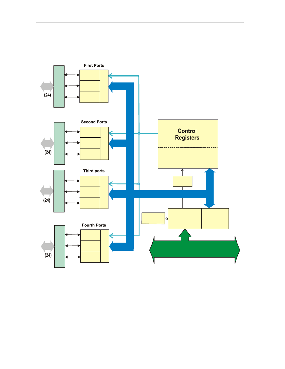
Block Diagram
PCI-QUAD-AC5 functions are illustrated in the block diagram shown here.
PCI
Controller
BADR2
Boot
EEPROM
Decode/Status
Bus
Timing
Controller FPGA and Logic
Local Bus
PCI Bus (5V, 32-BIT, 33MHZ)
Control
Bus
Port A
Port B
C
ont
ro
l
A(7:0)
B(7:0)
Port C
C(7:0)
S
S
R
-P
B
24
AC/DC
Port A
Port B
Co
nt
ro
l
A(7:0)
B(7:0)
Port C
C(7:0)
S
S
R
-P
B
24
AC/DC
I/O Module
Racks
Port A
Port B
Con
tr
o
l
A(7:0)
B(7:0)
Port C
C(7:0)
S
S
R
-P
B
24
AC/DC
Port A
Port B
Con
tr
o
l
A(7:0)
B(7:0)
Port C
C(7:0)
S
S
R
-P
B
24
AC/DC
I/O Module
Racks
1-2