FUJITSU MB39A104 User Manual
Page 7
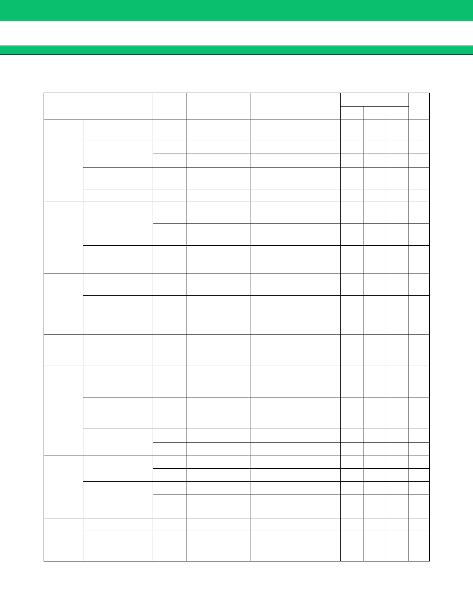
MB39A104
7
(Continued)
(VCC
= VCCO = 12 V, VREF = 0 mA, Ta = +25 °C)
*: Standard design value.
Parameter
Symbol
Pin No.
Conditions
Value
Unit
Min
Typ
Max
7.Error amplifier
block
[Er
ro
r Amp1
,
Error
Amp2]
Frequency
bandwidth
BW
9, 16
A
V
= 0 dB
⎯
1.6*
⎯ MHz
Output voltage
V
OH
9, 16
⎯
4.7
4.9
⎯
V
V
OL
9, 16
⎯
⎯
40
200
mV
Output source
current
I
SOURCE
9, 16
FB1
= FB2 = 2 V
⎯
−2
−1
mA
Output sink current
I
SINK
9, 16
FB1
= FB2 = 2 V
150
200
⎯
µA
8.
PWM
com
par
at
or
blo
c
k
[P
WM
Co
m
p
.1
,
PW
M Co
mp
.2
]
Threshold voltage
V
T0
6, 19
Duty cycle
= 0 %
1.4
1.5
⎯
V
V
T100
6, 19
Duty cycle
= Dtr
⎯
2.5
2.6
V
Input current
I
DTC
6, 19
DTC1
= DTC2 = 0.4 V
−2.0 −0.6
⎯
µA
9.
Over
curr
en
t
pr
ot
ect
ion
circu
it
blo
c
k
[O
CP1
, OC
P2]
ILIM terminal input
current
I
LIM
5, 20
R
T
= 24 kΩ, C
T
= 100 pF
99
110
121
µA
Offset voltage
V
IO
5, 20
⎯
⎯
1*
⎯
mV
10
.B
ia
s
volt
age
blo
c
k
[VH]
Output voltage
V
H
2
VCC
= VCCO = 7 V to 19 V
VH
= 0 mA to 30 mA
V
CC
−
5.5
V
CC
−
5.0
V
CC
−
4.5
V
11
.O
ut
put
blo
c
k
[Drive1, Drive2]
Output source
current
I
SOURCE
3, 22
OUT1 to OUT4
= 7 V,
Duty
≤ 5 %
(t
= 1/f
OSC
×Duty)
⎯
−300
⎯
mA
Output sink current
I
SINK
3, 22
OUT1 to OUT4
= 12 V,
Duty
≤ 5 %
(t
= 1/f
OSC
×Duty)
⎯
350
⎯
mA
Output ON
resistor
R
OH
3, 22
OUT1
= OUT2 = −45 mA
⎯
8.0
12.0
Ω
R
OL
3, 22
OUT1
= OUT2 = 45 mA
⎯
6.5
9.7
Ω
12
.Con
tr
ol block
[CTL
]
CTL input voltage
V
IH
24
IC Active mode
2
⎯
19
V
V
IL
24
IC Standby mode
0
⎯
0.8
V
Input current
I
CTLH
24
CTL
= 5 V
⎯
50
100
µA
I
CTLL
24
CTL
= 0 V
⎯
⎯
1
µA
13
.G
ene
ra
l
Standby current
I
CCS
1, 17
CTL
= 0 V
⎯
0
10
µA
Power supply
current
I
CC
1, 17
CTL
= 5 V
⎯
4.0
6.0
mA