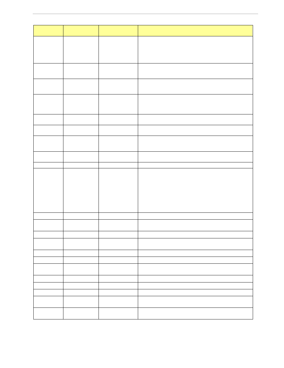
Table 3-2: 71m6533-db demo board description – Maxim Integrated 71M6533-DB User Manual
Page 56
71M6533-
DB Demo Board User’s Manual
Page: 56 of 75
`
REV 3
Item #
Reference
Designator
Name
Use
12
J12
OPT_RX, VBAT,
OPT_TX, GND
Five-pin header for access to the optical port (UART1).
Terminal 2 monitors the TX_OPT output of the IC. Terminal
4 monitors the OPT_RX input to the IC.
No jumper should be place across VBAT and
OPT_TX_OUT
13
J1
5 Volt external
supply
Plug for connecting the external 5 VDC power supply.
14, 20, 24,
32
TP13, TP14,
TP15, TP16
GND
GND test points.
15
JP20
--
Two-pin header for selecting the signal for the pulse LED
(D6). With a jumper between pins 1 and 2, RPULSE is
selected. Pins 2 and 3 select YPULSE.
16
D6
VARS
VARh pulse LED.
17
TP21
--
Two-pin header providing access to the signals powering
the RPULSE LED (D5).
18
JP19
SEG21/DIO08
Two-pin header for selecting the signal for the pulse LED
(D5). With a jumper between pins 1 and 2, WPULSE is
selected. Pins 2 and 3 select XPULSE.
19
TP20
--
Two-pin header providing access to the signals powering
the WPULSE LED (D6).
21
D5
WATTS
Wh pulse LED.
22
JP16
BAT MODE
Selector for the operation of the IC when main power is re-
moved. A jumper across pins 2-3 (default) indicates that no
external battery is available. The IC will stay in brownout
mode when the system power is down and it will communi-
cate at 9600bd. A jumper across pins 1-2 indicates that an
external battery is available. The IC will be able to trans-
ition from brownout mode to sleep and LCD modes when
the system power is down and it will communicate at
300bd.
23
JP6
DIO03_R
Three-pin header providing access to DIO03.
25
JP7
ICE_EN
To enable the ICE interface a jumper is installed across
pins 2 and 3.
26
U8
--
LCD display
– eight digits, 14 segments.
27
JP13, JP14,
JP15
DIO56, DIO57,
DIO58
Two-pin headers providing access to the DIO signals
DIO56, DIO57, and DIO58.
28
J2
DEBUG
Connector for USB-Serial Adapter. 2x8 pin male header.
29
U5
--
The IC 71M6533 soldered to the PCB.
30
TP8
CKTEST,
TMUXOUT
Test points for access to the CKTEST and TMUXOUT pins
on the IC.
31
TP17
VREF
Test point for access to the VREF pin on the IC.
33
TP10
V1_R
Three-pin header for control of the V1 input to the IC.
34
J18
--
SPI interface connector.
35, 39, 41,
43
J19, J20, J21,
J22
IAN/IAP, IBN/IBP,
ICN/ICP, IDP
Two-pin headers for monitoring the current channel inputs.
36
J14
EMULATOR I/F
2x10 emulator connector port for the Signum ICE ADM-51
or for the TFP2 Flash Programmer.
Table 3-2: 71M6533-DB Demo Board Description