Intel 80L186EA User Manual
Page 28
80C186EA 80C188EA 80L186EA 80L188EA
AC SPECIFICATIONS
AC Characteristics
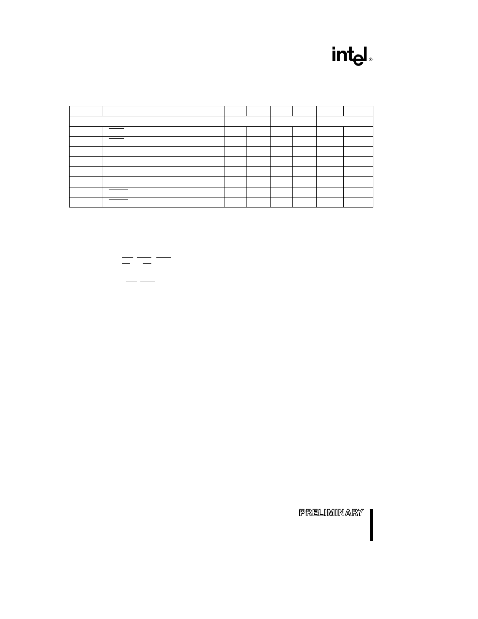
80L186EA13 80L186EA8
Symbol
Parameter
Min
Max
Min
Max
Units
Notes
SYNCHRONOUS INPUTS
13 MHz
8 MHz
T
CHIS
TEST NMI INT3 0 T1 0IN ARDY
22
22
ns
1 9
T
CHIH
TEST NMI INT3 0 T1 0IN ARDY
3
3
ns
1 9
T
CLIS
AD15 0 (AD7 0) ARDY SRDY DRQ1 0
22
22
ns
1 10
T
CLIH
AD15 0 (AD7 0) ARDY SRDY DRQ1 0
3
3
ns
1 10
T
CLIS
HOLD
22
22
ns
1 9
T
CLIH
HOLD
3
3
ns
1 9
T
CLIS
RESIN (to CLKIN)
22
22
ns
1 9
T
CLIH
RESIN (from CLKIN)
3
3
ns
1 9
NOTES
1 See AC Timing Waveforms for waveforms and definition
2 Measured at V
IH
for high time V
IL
for low time
3 Only required to guarantee I
CC
Maximum limits are bounded by T
C
T
CH
and T
CL
4 Specified for a 50 pF load see Figure 13 for capacitive derating information
5 Specified for a 50 pF load see Figure 14 for rise and fall times outside 50 pF
6 See Figure 14 for rise and fall times
7 T
CHOV1
applies to BHE (RFSH) LOCK and A19 16 only after a HOLD release
8 T
CHOV2
applies to RD and WR only after a HOLD release
9 Setup and Hold are required to guarantee recognition
10 Setup and Hold are required for proper operation
11 T
CHOVS
applies to BHE (RFSH) and A19 16 only after a HOLD release
12 Pin names in parentheses apply to the 80C188EA 80L188EA
28
28