Power supply, Block diagram, Intelligent character display and721gst/gst-led – Purdy AND721GST/GST-LED User Manual
Page 2
Intelligent Character Display
AND721GST/GST-LED
Purdy Electronics Corporation • 720 Palomar Avenue • Sunnyvale, CA 94085
7-27-99
Tel: 408.523.8200 • Fax: 408.733.1287 •
• www.purdyelectronics.com
2
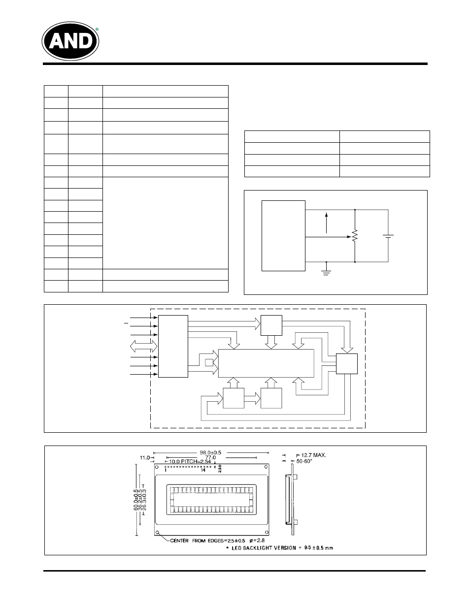
Power Supply
The LCD panel is driven by the voltage V
DD
–V
O
, so an
adjustable V
O
is required for contrast control and
temperature compensation.
Power Supply Block Diagram
Block Diagram
Dimensional Outline
1
GND
Ground
2
V
DD
+5 Power Supply
3
V
O
LCD Drive Voltage
4
RS
“H” Data Input
“L” Command Input
5
R/W
Read/Write
6
E
Enable
7
DB0
Data Bus
DB0-DB7 are for 8-bit operation
DB4-DB7 are for 4-bit operation
8
DB1
9
DB2
10
DB3
11
DB4
12
DB5
13
DB6
14
DB7
15
LED
LED Anode (+)
16
LED
LED Cathode Ground
Connector Pin Assignment
Pin #
Signal
Function
Temperature Variations
Temperature
V
DD
–V
O
0°C
5.00
+25°C
4.75
+50°C
4.50
V
DD
V
O
GND
V
DD
– V
O
V
DD
– V
O
= LCD Drive Voltage
VR10 to 20 k
Ω
VR
V
DD
(+5V)
Driver
Driver
Driver
Driver
Controller/
Driver
16
16
16
40
4
4
40
40
40
20
4
20
LCD
E
R/W
RS
V
DD
V
O
GND
DBO-DB7
8
Connector Pin Assignment