Universal serial bus microcontroller – EMC EM78612 User Manual
Page 12

EM78612
Universal Serial Bus Microcontroller
10 •
•••
Product Specification(V1.0) 03.22.2006
(This specification is subject to change without further notice)
R0 (Indirection Addressing Register)
R1 (Time Clock / Counter Register)
R2 (Program Counter) & Stack
R3 (Status Register)
R4 (RAM Select Register)
R5 (Data line I/O Register)
R6 (Port 6 I/O Register)
R7 (Port 7 I/O Register)
R8 (Port6 wakeup pin selection Register)
R9 (Port7 wakeup pin selection Register)
RC (USB Application Status Register)
RD (USB Application FIFO address register)
RE (USB Application FIFO data register)
RF (Interrupt Status Register)
00
01
02
03
04
05
06
07
08
General Purpose Register
09
0C
0D
0F
0E
IOC5 (Port 5 I/O Control Register)
IOC6 (Port 6 I/O Control Register)
IOC7 (Port 7 I/O Control Register)
IOC8 (Sink Curent Control Register)
IOCA (Operation mode Control Register)
IOCB (Port 6 pull low Control Register)
IOCC (Port 6 pull high Control Register)
IOCD (Port 7 pull high Control Register)
IOCE (Special Function Control Register)
IOCF (Interrupt Mask Register)
EP0's FIFO
EP1's FIFO
Data Byte Pointer of EP0
00
01
10
1F
20
General Purpose
Registers
(Bank0)
General Purpose
Registers
(Bank1)
3F
Data Byte Pointer of EP1
11
✣✘✤✦✥
✧✩★
✣✘✤✦✥
✧✩★
✣✘✤✦✥
✧✩★
✣✘✤✦✥
✧✩★
✣✘✤✦✥
✧✆✪
✣✘✤✦✥
✧✆✪
✣✘✤✦✥
✧✆✪
✣✘✤✦✥
✧✆✪
✣✘✤✦✥
✧✦✫
✣✘✤✦✥
✧✦✫
✣✘✤✦✥
✧✦✫
✣✘✤✦✥
✧✦✫
✣✘✤✦✥
✧✦✬
✣✘✤✦✥
✧✦✬
✣✘✤✦✥
✧✦✬
✣✘✤✦✥
✧✦✬
✣✘✤✦✥
✧✢✭
✣✘✤✦✥
✧✢✭
✣✘✤✦✥
✧✢✭
✣✘✤✦✥
✧✢✭
✣✘✤✦✥
✧✦✮
✣✘✤✦✥
✧✦✮
✣✘✤✦✥
✧✦✮
✣✘✤✦✥
✧✦✮
✣✘✤✦✥
✧✦✯
✣✘✤✦✥
✧✦✯
✣✘✤✦✥
✧✦✯
✣✘✤✦✥
✧✦✯
✣✘✤✦✥
✧✩✰
✣✘✤✦✥
✧✩✰
✣✘✤✦✥
✧✩✰
✣✘✤✦✥
✧✩✰
10
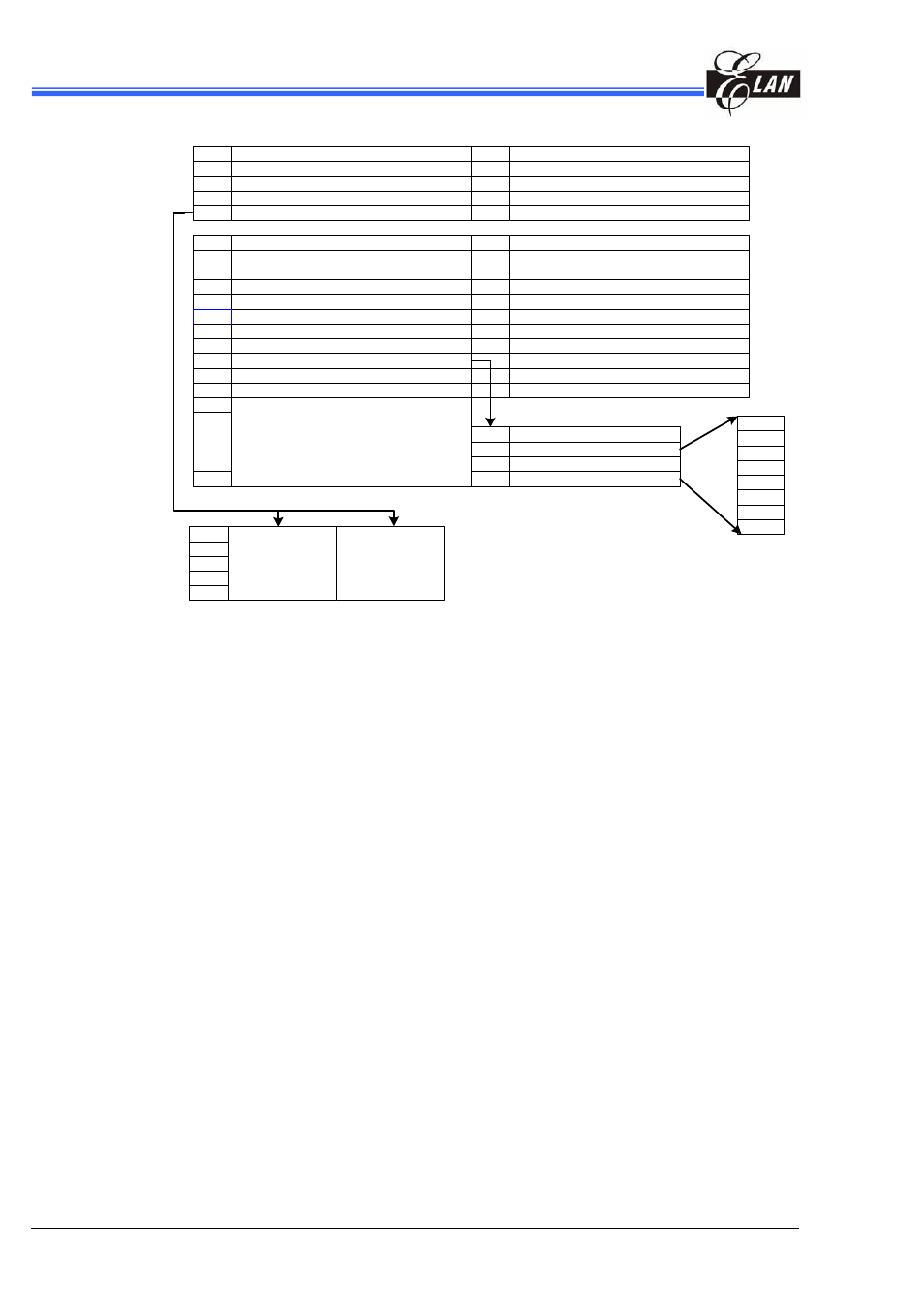
Fig 7-1 The Organization of EM78612 Data RAM
7.2.1.1 Operation Registers in Bank 0
The following introduces each of the Operation Registers under the Special Purpose
Registers. The Operation Registers are arranged according to the order of registers’
address. Note that some registers are read only, while others are both readable and
writable.
R0 (Indirect Address Register)
Default Value: (0B_0000_0000)
R0 is not a physically implemented register. Its major function is to be an indirect
address pointer. Any instruction using R0 as a pointer actually accesses the data
pointed by the RAM Select Register (R4).
R1 (Time / Clock Counter)
Default Value: (0B_0000_0000)
This register TCC, is an 8-bit timer or counter. It is readable and writable as any other
register. The Timer module will increment every instruction cycle . The user can work
around this by writing an adjusted value. The Timer interrupt is generated when the R1
register overflows from FFh to 00h. This overflow sets bit TCIF(RF[0]). The interrupt
can be masked by clearing bit TCIE (IOCF[0]).After Power-on reset and WatchDog
reset, the initial value of this register is 0x00.
