Pin assignments, Pin descriptions, Module description – Linx Technologies TXM-xxx-ES User Manual
Page 6
– –
– –
6
7
Pin Assignments
Figure 9: ES Series Transmitter Pinout (Top View)
Pin Descriptions
Pin Number
Name
I/O Description
1
PDN
I
Power Down. Pulling this line low places
the transmitter into a low-current state. The
module is not able to transmit a signal in this
state.
2
LADJ
I
Level Adjust. This line can be used to adjust
the output power level of the transmitter.
Connecting to V
CC
gives the highest output,
while placing a resistor to GND lowers the
output level (see Figure 5 on page 4).
3
V
CC
—
Supply Voltage
4
GND
—
Analog Ground
5
DATA
O
Analog or Digital Data Input
6
/CLK
O
Divided Clock Output
7
/CLK SEL
O
Clock Frequency Selection. Logic low
selects divide by 256, logic high selects
divide by 1,024.
8
LO_V_D
O
Low Voltage Detect. This line goes low when
V
CC
is less than 2.15V.
9
GND
—
Analog Ground
10
ANT
—
50-ohm RF Output
Pin Descriptions
Figure 10: ES Series Transmitter Pin Descriptions
PDN
LADJ
VCC
LO_V_D
/CLK SEL
/CLK
GND
DATA
ANT
GND
1
2
3
4
5
6
7
8
9
10
Module Description
The TXM-***-ES module is a single-channel transmitter designed for
the wireless transfer of digital or analog information over distances of
up to 1,000 feet outdoors and up to 500 feet indoors. It is based on a
high-performance synthesized architecture. FM / FSK modulation is utilized
to provide superior performance and noise immunity over AM-based
solutions. The ES Series is incredibly compact and cost-effective when
compared with other FM / FSK devices. Best of all, it is packed with many
useful features and capabilities that offer a great deal of application flexibility
to the designer. Some of these features are:
/CLK Output (use for an external micro-controller)
LO_V_DET (low-voltage detection)
LADJ (adjust the RF output power)
The ES Series is offered in the 902 to 928MHz band, which is free from the
legal restrictions of the lower 260 to 470MHz band. This gives the designer
much more freedom in the types of applications that can be designed. The
869.85MHz version allows for the same freedom of design in European
applications.
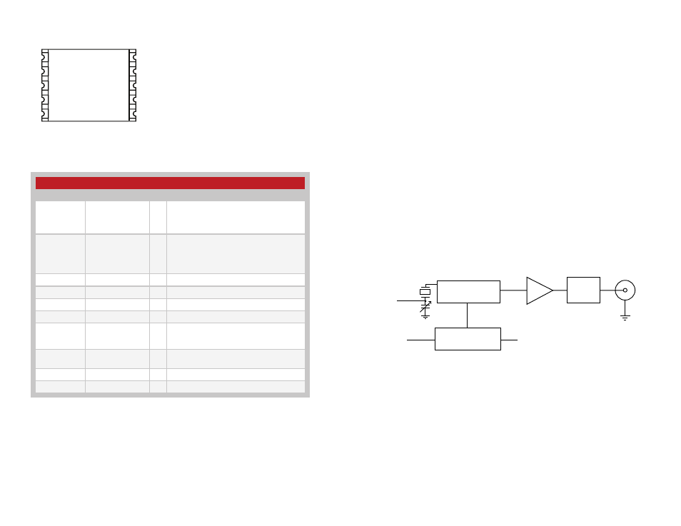
Figure 11: ES Series Transmitter Block Diagram
Precision
Crystal
Data In
/CLK SEL
/CLK Output
PLL Frequency
Synthesizer
Frequency Divider
256 / 1,024
LC
Filter
RF Amplifier
Antenna Port