Ordering information, Absolute maximum ratings, Electrical specifications – Linx Technologies TXM-xxx-ES User Manual
Page 4: Electrical specifications ordering information
– –
– –
2
3
ES Series Transmitter Specifications
Parameter
Symbol
Min.
Typ.
Max.
Units
Notes
Power Supply
Operating Voltage
V
CC
2.1
3.0
4.0
VDC
Supply Current
I
CC
5.5
7.0
8.5
mA
Power-Down Current
I
PDN
90.0
µA
7
Transmit Section
Transmit Frequency
F
C
TXM-916-ES
916.48
MHz
4
TXM-869-ES
869.85
MHz
4
Electrical Specifications
Ordering Information
Ordering Information
Part Number
Description
TXM-869-ES
ES Series Transmitter 869MHz
TXM-916-ES
ES Series Transmitter 916MHz
RXM-869-ES
ES Series Receiver 869MHz
RXM-916-ES
ES Series Receiver 916MHz
EVAL-***-ES
Basic Evaluation Kit
MDEV-***-ES
Master Development System
*** = Frequency
Receivers are supplied in tubes of 40 pcs.
Figure 2: Ordering Information
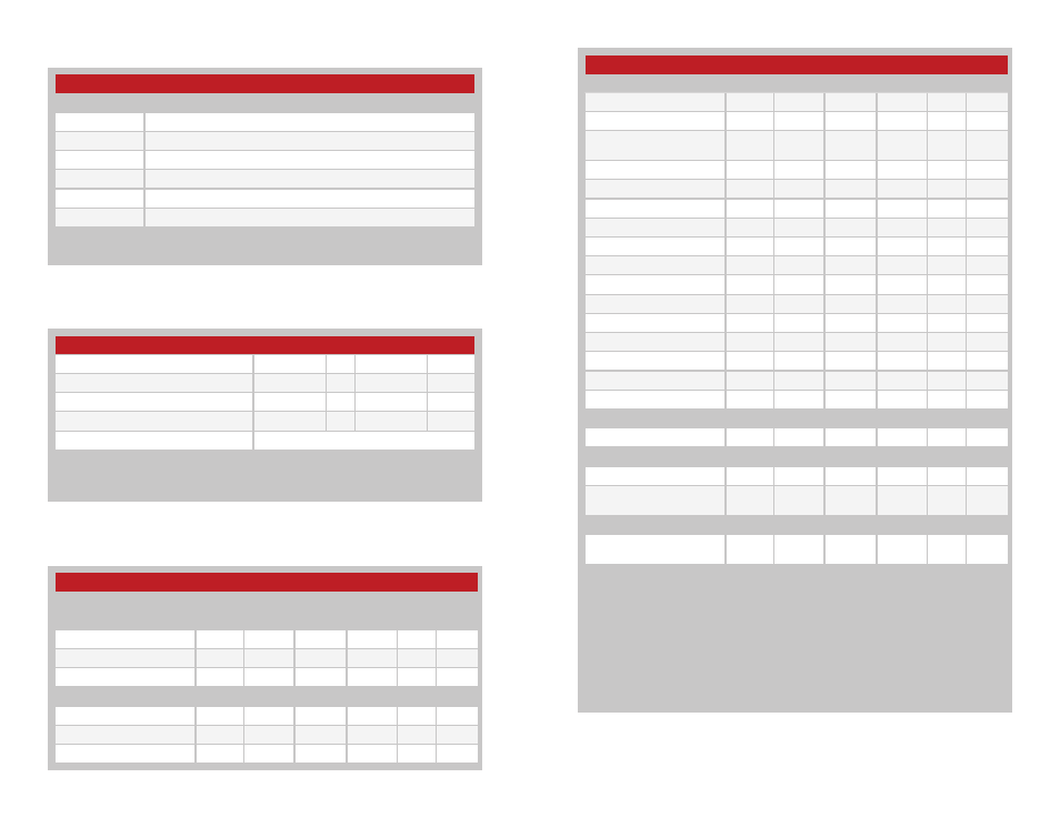
ES Series Transmitter Specifications
Parameter
Symbol
Min.
Typ.
Max.
Units
Notes
Center Frequency Accuracy
–60
+60
kHz
1
Output Power
P
O
–3
0
+4
dBm
2,3
Output Power Control
Range
65
dB
2,3,7
Harmonic Emissions
P
H
–55
–47
dBc
2
Frequency Deviation
F
DEV
TXM-916-ES
80
130
kHz
5
TXM-868-ES
70
130
kHz
5
Data Rate
200
56,000
bps
7
Analog/Audio Bandwidth
20
28,000
Hz
6,7
Data Input
Logic Low
V
IL
0.0
0.4
VDC
8
Logic High
V
IH
3.0
5.2
VDC
8
Power-Down Input
Logic Low
0.0
0.7
VDC
Logic High
1.5
V
CC
VDC
Analog Input
0.0
5.0
V
P-P
9
Antenna Port
RF Output Impedance
R
OUT
50
Ω
7
Timing
Transmitter Turn-On Time
0.1
0.5
1.5
ms
7,10
Max. Time Between
Transitions
5.0
ms
7,11
Environmental
Operating Temperature
Range
0
+70
ºC
7
1. Center frequency measured while
modulated with a 0-5V square wave
2. Into a 50-ohm load
3. LADJ open
4. Maximum power when LADJ open,
minimum power when LADJ grounded
5. DATA pin modulated with a 0-5V
square wave
6. The audio bandwidth is wide to
accommodate the needs of the data
slicer
7. Characterized, but not tested
8. The ES is optimized for both 0-5V and
0-3V modulation when sending digital
data
9. Analog signals, including audio, should
be AC-coupled
10. Time to transmitter readiness from the
application of power to V
CC
or PDN
going high
11. Maximum time without a data transition
Figure 4: Electrical Specifications
Absolute Maximum Ratings
Supply Voltage V
cc
−0.3
to
+4.0
VDC
Any Input or Output Pin
−0.5
to
V
CC
+ 0.5
VDC
Operating Temperature
0
to
+70
ºC
Storage Temperature
–40
to
+90
ºC
Soldering Temperature
255ºC for 10 seconds
Exceeding any of the limits of this section may lead to permanent damage to the device.
Furthermore, extended operation at these maximum ratings may reduce the life of this
device.
Absolute Maximum Ratings
Figure 3: Absolute Maximum Ratings