Pin assignments, Pin descriptions – Linx Technologies TRM-xxx-LT User Manual
Page 7
– –
– –
8
9
1. 200mV/div
2. 2.00V/div
200µS/div
1
2
PDN
Carrier
Figure 14: TX Turn-On Time from PDN
1. 200mV/div
2. 2.00V/div
1.00mS/div
1
2
Vcc
Carrier
Figure 15: TX Turn-On Time from V
CC
1. 200mV/div
2. 2.00V/div
5.00µS/div
1
2
DATA
Carrier
Figure 16: TX Turn-Off Time
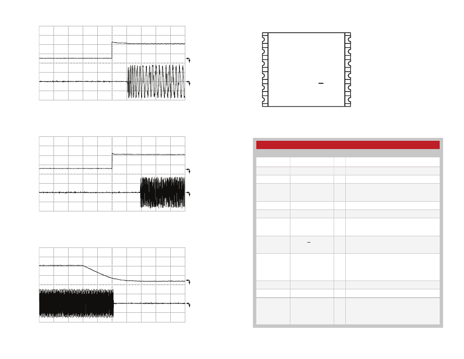
Pin Assignments
ANT
GND
NC
GND
PDN
T/R SEL
DATA
RSSI
A REF
ANALOG
LADJ
VCC
1
2
3
4
5
6
7
8
9
10
11
12
Figure 17: LT Series Transceiver Pinout (Top View)
Pin Descriptions
Figure 18: LT Series Transceiver Pin Descriptions
Pin Descriptions
Pin Number
Name
I/O Description
1
ANT
—
50
Ω
RF Port
2
GND
—
Analog Ground
3
NC
—
No Connection
4
RSSI
O
Received Signal Strength Indicator. This line
will supply an analog voltage proportional to
the received signal strength.
5
A REF
O
Analog RMS (Average) Voltage Reference
6
ANALOG
O
Recovered Analog Output
7
DATA
I/O
Digital Data Line. This line outputs the
received data when in Receive Mode and is
the data input when in Transmit Mode.
8
T/R_SEL
I
Transmit/Receive Select. Pull this line low to
place the transceiver into receive mode. Pull
high to place into transmit mode.
9
PDN
I
Power Down. Pull this line low or leave
floating to place the receiver into a
low-current state. The module is not be able
to send or receive a signal in this state. Pull
high to activate the transceiver.
10
GND
—
Analog Ground
11
V
CC
—
Supply Voltage
12
LADJ/V
CC
I
Level Adjust. This line is used to adjust
the output power level of the transmitter.
Connecting to V
CC
gives the highest output,
while placing a resistor to V
CC
lowers the
output level (see Figure 5).