Typical performance graphs – Linx Technologies TRM-xxx-LT User Manual
Page 5
– –
– –
4
5
LT Series Transceiver Specifications Continued
Parameter
Symbol
Min.
Typ.
Max.
Units
Notes
Transmitter Section
Output Power
P
O
+9.2
+11
dBm
1,6
With a 750
Ω resistor
on LADJ
P
O
–4
0.0
4
dBm
2,6
Output Power Control
Range
–30
MAX
dB
9
Harmonic Emissions
P
H
–36
dBc
6
Antenna Port
RF Input Impedance
R
IN
50
Ω
9
Timing
Receiver Turn-On Time
Via V
CC
2.2
ms
8,9
Via PDN
0.25
ms
8,9
Max. Time Between
Transitions
15.0
ms
9
Transmtiter Turn-On Time
Via V
CC
2.0
ms
9
Via PDN
500
µs
9
Modulation Delay
30.0
ns
9
Transmit to Receive
Switch Time
180
400
µs
9
Receive to Transmit
Switch Time
490
1000
µs
9
Dwell Time
290
µs
9,11
Environmental
Operating Temperature
Range
–40
+85
ºC
9
1. With a 0
Ω resistor on LADJ
2. With a 750
Ω resistor on LADJ
3. I
SINK
= 500µA
4. I
SOURCE
= 500µA
5. I
SINK
= 20µA
6. Into a 50
Ω load
7. With a 50% square wave at 1,000bps
8. Time to valid data output
9. Characterized, but not tested
10. Receive Mode on power down (see
Using the PDN Line section)
11. Minimum time before mode change
Figure 4: Electrical Specifications
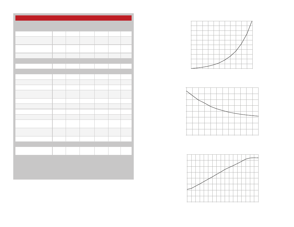
Typical Performance Graphs
0
1
2
3
4
5
6
7
8
9
10
12.00
9.00
6.00
3.00
0.00
-3.00
-6.00
-9.00
-12.00
-15.00
-18.00
-21.00
Output Power (dBm)
LADJ Resistance (k
Ω
)
Figure 5: Output Power vs. LADJ Resistance
0
2
4
6
8
10
12
14
16
10
8
6
4
2
0
-2
-4
-6
-8
-10
-12
-14
Output Power (dBm)
Supply Current (mA
)
Figure 6: Output Power vs. Current Consumption
0
0.2
0.4
0.6
0.8
1
1.2
1.4
1.6
-115 -110 -105 -100
-95
-90
-85
-80
-75
-70
-65
-60
-55
-50
-45
-40
-35
-30
RF IN (dBm)
VRSSI (V)
Figure 7: RSSI Curve