Pcb footprint, Board layout guidelines, Schematic diagram – Linx Technologies EVM-915-DTS User Manual
Page 5: Pcb footprint board layout guidelines
–
–
–
–
5
4
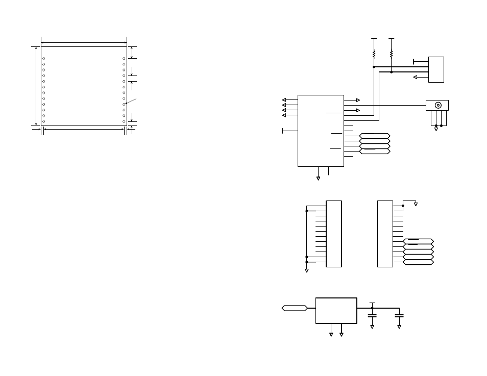
PCB Footprint
Board Layout Guidelines
The module’s design makes integration straightforward; however, it
is still critical to exercise care in PCB layout. Failure to observe good
layout techniques can result in a significant degradation of the module’s
performance. Grounding, filtering, decoupling, routing and PCB stack-up
are all important considerations for any RF design. Some basic design
guidelines are provided here.
The module should, as much as reasonably possible, be isolated from
other components on your PCB, especially high-frequency circuitry such as
crystal oscillators, switching power supplies, and high-speed bus lines.
When possible, separate RF and digital circuits into different PCB regions.
Make sure internal wiring is routed away from the module and antenna and
is secured to prevent displacement.
Bypass caps should be low ESR ceramic types and located directly
adjacent to the pin they are serving.
In some instances, a designer may wish to encapsulate or “pot” the
product. Since such compounds can considerably impact RF performance
and the ability to rework or service the product, it is the responsibility of the
designer to evaluate and qualify the impact and suitability of such materials.
Schematic Diagram
1
24
0.10”
(2.54)
Ø0.04” x 24
(1.02)
0.7”
(1.78)
0.208”
(5.28)
1.50”
(38.10)
1.38”
(35.05)
1.40”
(35.56)
0.05”
(1.27)
0.05”
(1.27)
3
+
3
4
5
6
7
8
9
10
11
12
13
14
1
2
3
4
5
6
7
8
9
10
11
12
JP1
1
2
3
4
5
6
7
8
9
10
11
12
JP2
GND
GND
J1
GND
3.3V
IN
1
GND
2
GND
T
OUT
U1
GNDGND
VCC
C1
GND
C2
GND
VIN
VIN
GND
1
NC
2
GND
15
GND
16
GND
17
GND
18
VCC
19
MOD1
CTS
CMD
TXD
RXD
GND
1
2
3
4
JP3
1K
R2
1K
R1
VCC
VCC
RESET
NC
CMD
RXD
TXD
CTS
NC
NC
C2D
GND
ANT
GND
GND
GND
GND
GND
GND
VCC
GND
GND
VCC
TXD
RXD
CMD
CTS
Figure 6: DTS Series EVM Module PCB Footprint
Figure 7: DTS Series EVM Module Schematic