Architecture – Sundance SMT8101 User Manual
Page 7
Version 1.3
Page 7 of 16
SMT8101 User Manual
Architecture.
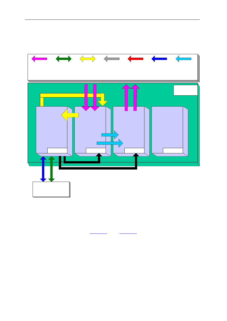
The following diagram shows the architecture of the SMT8101 system:
``
SMT391-VP
1-GHz ADC
Module
Module #2
Spare
SMT310Q
PC
Host
Data
SDB
Connection
Control
Comport
Data
Comport
Analogue
Connection
RSL Link
2.5Gbits/s
TIM site 2
TIM site 4
Data
SHB
Connection
Data
Global Bus
Connection
SMT381-VP
1-GHz DAC
Module
Module #3
TIM site 3
TIM site 1
SMT395
1-GHz DSP
Module
Module #1
SMT516
TIM site 1
SMT526
Control and Configuration Comports
SMT511
SMT522
SM
T
5
06
S
M
T
5
0
6
SM
T5
0
6
S
M
T
5
0
6
The SMT395-VP is the module that controls all operations of the system, starting
from configuring SMT391-VP and SMT381-VP FPGAs (Xilinx Virtex-II Pro VP30-6)
using configuration ports (Comports).
The data path is clearly as follows: Analog inputs are fed into the ADC module that
converts it into digital samples. The data flow is then passed onto the DAC module
signals. Data streams go through 2 FPGAs where processing can be added.
Samples are originally coded on 8-bits by the ADCs, sent over the RSLs and
converted into a 14-bit format samples to match the DAC data input as follow:
Sample_DAC_14_bits = Sample_ADC_8_bit & "100000"
The SMT391-VP has an on-board VCO that is used to generate a 1GHz clock, which
is passed to the SMT381-VP so ADC and DAC channels are receiving the same