2 timing diagrams – Sundance SMT123-SHB User Manual
Page 8
User Guide SMT123-SHB
Page 8 of 13
11/06/2004
1.5.1 LED
Indicators
A bank of 8 LEDs is situated on the left edge of the board (as shown on the left of Figure 2),
which indicate that the board has power, and the status of the fibre link (blue LED).Table 1
below shows the arrangement of the LEDs, their meaning, and the FPGA pin with which they
are driven. Most of them are meant to help the users to debug their applications.
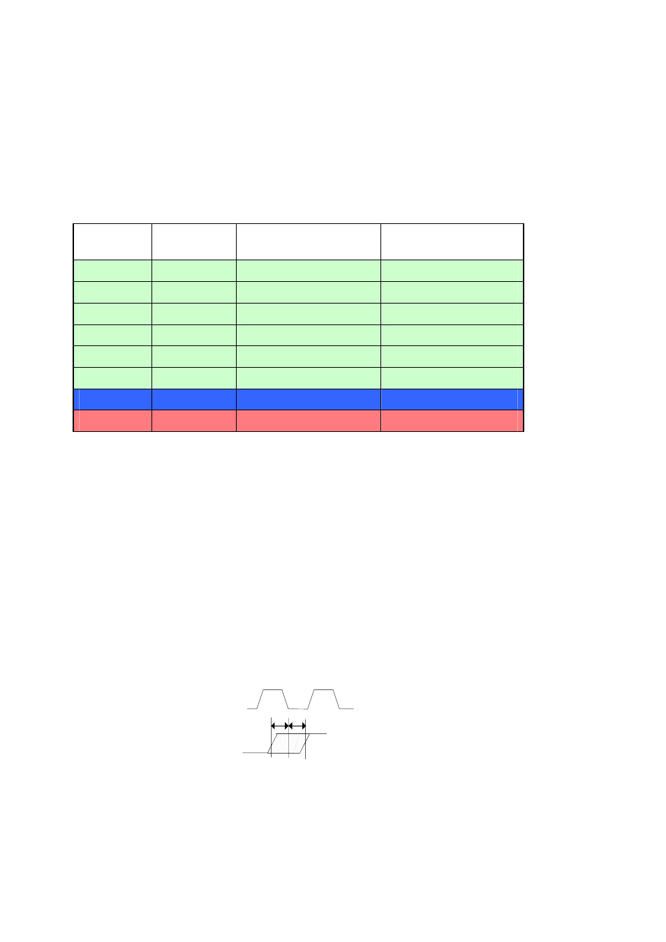
Reference Name
Meaning
FPGA pin that drives
it
D4
Cam1
USER defined
T10
D5
Cam2
USER defined
R10
D6
Cam3
USER defined
T9
D7
Cam4
USER defined
R9
D8
Cam5
USER defined
P9
D9
Cam6
USER defined
N9
D10
SMURF
Link valid
T3
D11
RUDOLPH
FPGA not programmed
N/A
Table 1 LEDs (the background of each row indicates the colour of the LED)
2 Timing
Diagrams
The VSC7146 needs to be provided with two separate clock signals: REF and TBC which
must not have their opposing edges coincident within 2.0 ns of each other as illustrated in
Figure 4. (T1 and T2 must be minimum 2ns). The REF signal comes straight to its
corresponding pin of the Vitesse chip from the crystal though a small resistor, whereas TBC
signal is the same clock passed through the Virtex II. It is connected to the pin N8 of the
FPGA and the delay may be adjusted by using the DRC characteristics of this chip.
REF
TBC
T1
T2
Figure 4 - TBC and REF Timing Waveforms