3 block diagram, 4 physical description, Functional description – Sundance SMT123-SHB User Manual
Page 6

User Guide SMT123-SHB
Page 6 of 13
11/06/2004
• Functional Description
1.3 Block
Diagram
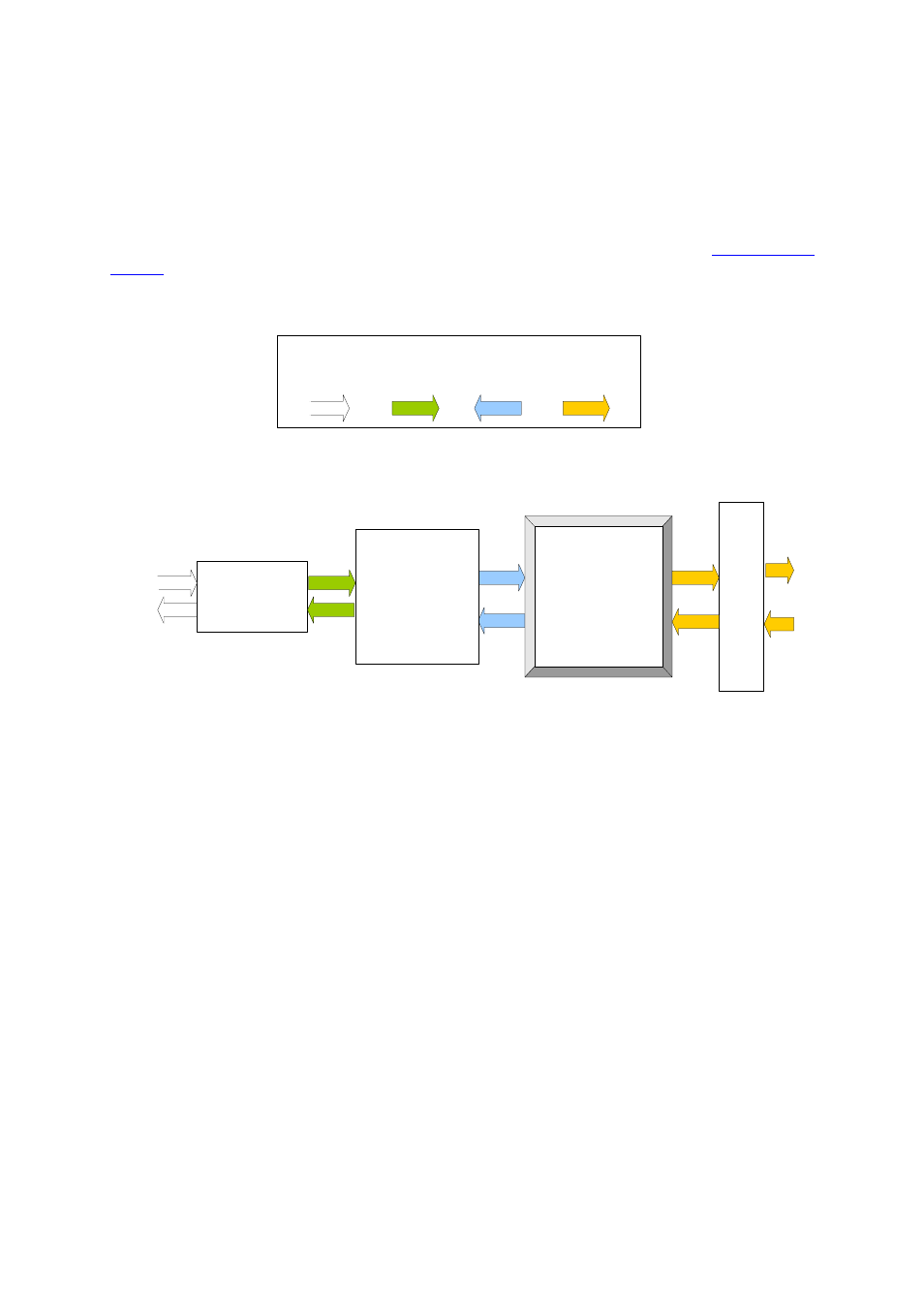
Figure 1 below shows the data-flow through the board. Serial data to and from the two Fibre
Channel connectors is passed through a Vitesse Semiconductor VSC7146 Serialiser /
Deserialiser IC, and then to or from the Xilinx Virtex-II FPGA, XC2V250–4)
Virtex-II Data
Sheets
on a pair of 20-bit busses. The FPGA codes the data in a 10b/8b format for
transmission through the fibre link and does the reverse on received data.
Industry Standard
Small Form-Factor
Fibre Channel module
S
H
B
C
o
n
n
e
c
t
o
r
+
-
+
-
20
/
20
/
Sundance SHB connector.
(Samtec QSH-030-01-L-D-A-K)
Xilinx
Virtex-II
Vitesse
VSC7146
20
/
20
/
Differential
2Gbit TX & RX
Pairs
+
-
20
/
20-bit
(2 x 10/8 coded)
TX/RX data
3.3v
SHB/SDB Data
Fibre Channel
IN/OUT
20
/
20
/
20
/
Figure 1 - Data Flow Diagram
1.4 Physical
Description
The board is 100mm x 100.4mm. The shape of the board is designed to fit into a PCI slot
although no physical connections to such bus are available. An industry standard “SFF”
(Small Form-Factor) Fibre Channel module is fitted onto the board and protrudes from the
front end for connection of the fibre cables. It uses the Industry Standard LC Optical
Connector. The board requires only 5V supplied through a 4-pin 0.1” header compatible with
standard floppy disk power connectors (J5). An on-board power conversion section derives
the other voltages required on the board, i.e. 3.3v and 1.5v.
1.4.1 Board
Layout
Figure 2 below shows the layout of the board. Throughout this document, wherever “left,
right, top or bottom” are referred to in reference to the card, it is assumed that the card is in
the orientation shown in this diagram.
