Chapter 3 – DFI HM960-HM86 User Manual
Page 24
www.dfi .com
Chapter 3 Hardware Installation
24
Chapter 3
ȟ
ȟ
ȟ
ȟ
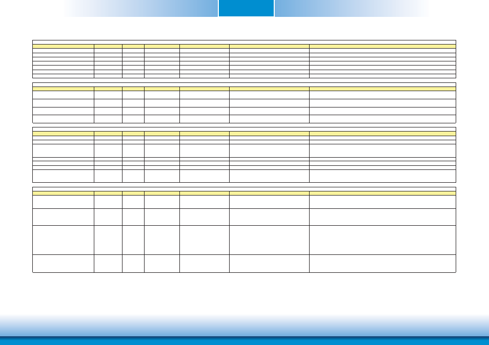
Signal
Pin#
Pin Type
Pwr Rail /Tolerance
HM960-QM87/HM86
Carrier Board
Description
VGA_RED
B89
O Analog
Analog
PD 150 TO GND
PD 150R,connect to VGA connector with EMI
Red for monitor. Analog output
VGA_GRN
B91
O Analog
Analog
PD 150 TO GND
PD 150R,connect to VGA connector with EMI
Green for monitor. Analog output
VGA_BLU
B92
O Analog
Analog
PD 150 TO GND
PD 150R,connect to VGA connector with EMI
Blue for monitor. Analog output
VGA_HSYNC
B93
O CMOS
3.3V / 3.3V
Connect to VGA connector with a3.3V Buffer
Horizontal sync output to VGA monitor
VGA_VSYNC
B94
O CMOS
3.3V / 3.3V
Connect to VGA connector with a 33V Buffer
Vertical sync output to VGA monitor
VGA_I2C_CK
B95
I/O OD CMOS 3.3V / 3.3V
PU 2.2K TO 3V3
Connect to VGA connector with a 3.3V to 5V
DDC clock line (I2C port dedicated to identify VGA monitor capabilities)
VGA_I2C_DAT
B96
I/O OD CMOS 3.3V / 3.3V
PU 2.2K TO 3V3
Connect to VGA connector with a 3.3V to 5V
DDC data line.
Signal
Pin#
Pin Type
Pwr Rail /Tolerance
HM960-QM87/HM86
Carrier Board
Description
SER0_TX
A98
O CMOS
3.3V/5V
PD 4.7K TO GND
General purpose serial port 0 transmitter
SER0_RX
A99
I CMOS
3.3V/5V
PU 47K TO 3V3
General purpose serial port 0 receiver
SER1_TX
A101
O CMOS
3.3V/5V
PD 4.7K TO GND
General purpose serial port 1 transmitter
SER1_RX
A102
I CMOS
3.3V/5V
PU 47K TO 3V3
General purpose serial port 1 receiver
Signal
Pin#
Pin Type
Pwr Rail /Tolerance
HM960-QM87/HM86
Carrier Board
Description
I2C_CK
B33
I/O OD CMOS 3.3V Suspend/3.3V
PU 2.2K TO 3V3_DU_EC
General purpose I2C port clock output
I2C_DAT
B34
I/O OD CMOS 3.3V Suspend/3.3V
PU 2.2K TO 3V3_DU_EC
General purpose I2C port data I/O line
SPKR
B32
O CMOS
3.3V / 3.3V
Output for audio enunciator - the "speaker" in PC-AT systems.
This port provides the PC beep signal and is mostly intended for
debugging purposes.
WDT
B27
O CMOS
3.3V / 3.3V
Output indicating that a watchdog time-out event has occurred.
FAN_PWNOUT
B101
O OD CMOS
3.3V / 12V
Fan speed control. Uses the Pulse Width Modulation (PWM) technique to control the fan's RPM.
FAN_TACHIN
B102
I OD CMOS
3.3V / 12V
PU 10K TO 3V3
Fan tachometer input for a fan with a two pulse output.
TPM_PP
A96
I CMOS
3.3V / 3.3V
PU 0 TO 3V3_DU
NC PU 4.7K TO 3V3_SB
Trusted Platform Module (TPM) Physical Presence pin. Active high.
TPM chip has an internal pull down. This signal is used to indicate
Physical Presence to the TPM.
Signal
Pin#
Pin Type
Pwr Rail /Tolerance
HM960-QM87/HM86
Carrier Board
Description
PWRBTN#
B12
I CMOS
3.3V Suspend/3.3V
PU 10K TO 3V3_DU_EC
PU 4.7K TO 3V3_SB
A falling edge creates a power button event. Power button events can
be used to bring a system out of S5 soft off and other suspend states,
as well as powering the system down.
SYS_RESET#
B49
I CMOS
3.3V Suspend/3.3V
PU 10K TO 3V3_DU
NC PU 4.7K TO 3V3_SB
Reset button input. Active low request for Module to reset and reboot.
May be falling edge sensitive. For situations when SYS_RESET# is
not able to reestablish control of the system, PWR_OK or a power
cycle may be used.
CB_RESET#
B50
O CMOS
3.3V Suspend/3.3V
Reset output from Module to Carrier Board. Active low. Issued by
Module chipset and may result from a low SYS_RESET# input, a low
PWR_OK input, a VCC_12V power input that falls below the minimum
specification, a watchdog timeout, or may be initiated by the Module
software.
PWR_OK
B24
I CMOS
3.3V / 3.3V
PU 10K TO 3V3
Power OK from main power supply. A high value indicates that the
power is good. This signal can be used to hold off Module startup to
allow Carrier based FPGAs or other configurable devices time to be
programmed.
Serial Interface Signals Descriptions
Miscellaneous Signal Descriptions
Power and System Management Signals Descriptions
VGA Signals Descriptions