ADLINK cBP-3062 User Manual
Page 46
36
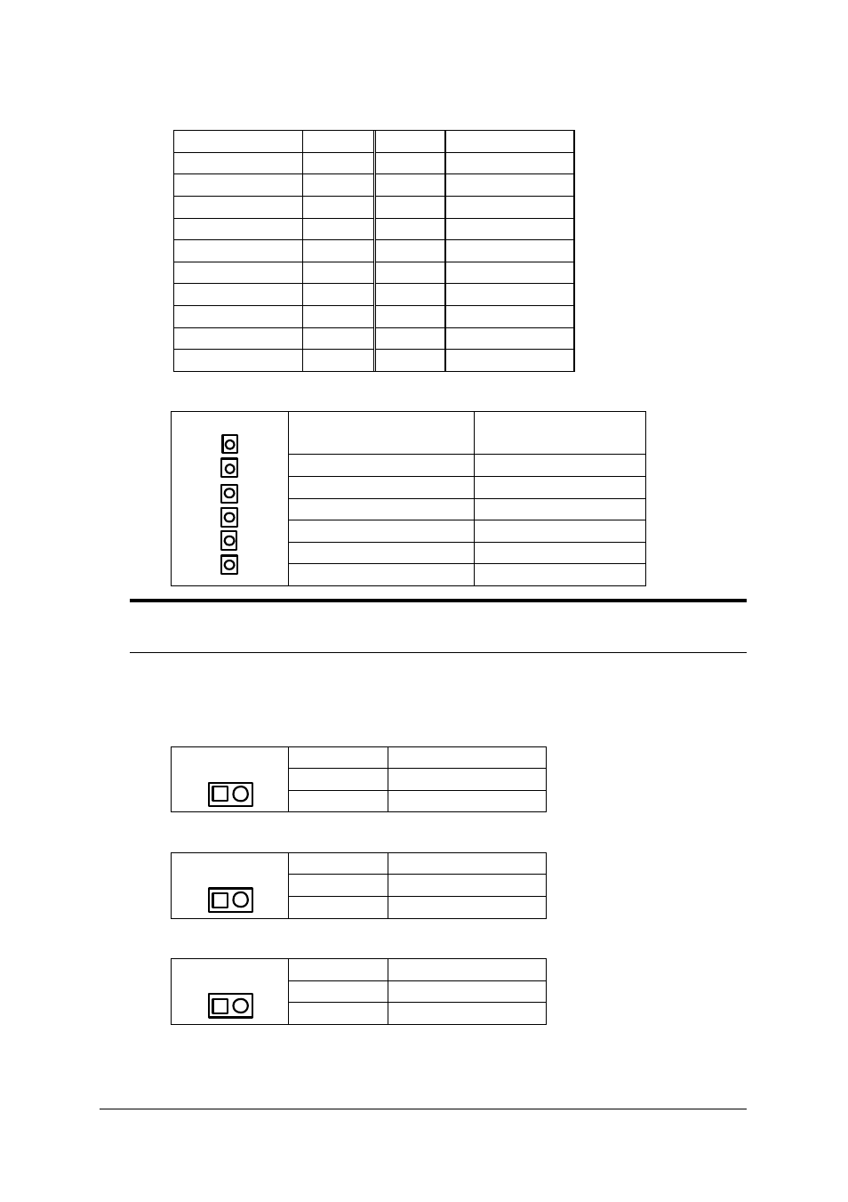
• Backplane
Signal
Pin No. Pin No.
Signal
+3.3V
1
11
+3.3V
+3.3V
2
12
-12V
GND
3
13
GND
+5V
4
14
INH#
GND
5
15
GND
+5V
6
16
+5V Sense-
GND
7
17
GND
FAL#
8*
18*
JP7
DEG#
9*
19
+5V Sense+
+12V
10
20
+5V
u
General Purpose screw terminals
Position
(from top to bottom)
Name
1
+3.3V
2
V(I/O)
3
+5V
4
GND
5
+12V
6
-12V
Note: that the V(I/O) must be shorted to either +3.3V or +5V. The default
factory setting is to shorted at +5V.
u
JP8 INH#: DC power inhibit signal
It is for inhibiting the ATX power supply. This connector is used for
power-on switch.
Pin #
Name
1
INH#
JP8
2
GND
u
JP9 RST#: System reset signal
Pin #
Name
1
RST#
JP9
2
GND
u
JP10 FAL#: Power supply fail input
Pin #
Name
1
FAL#
JP10
2
GND
This manual is related to the following products: