Operation theorem, Front connector pxi connector – ADLINK PXI-7901 User Manual
Page 17

Operation Theorem • 11
4
Operation Theorem
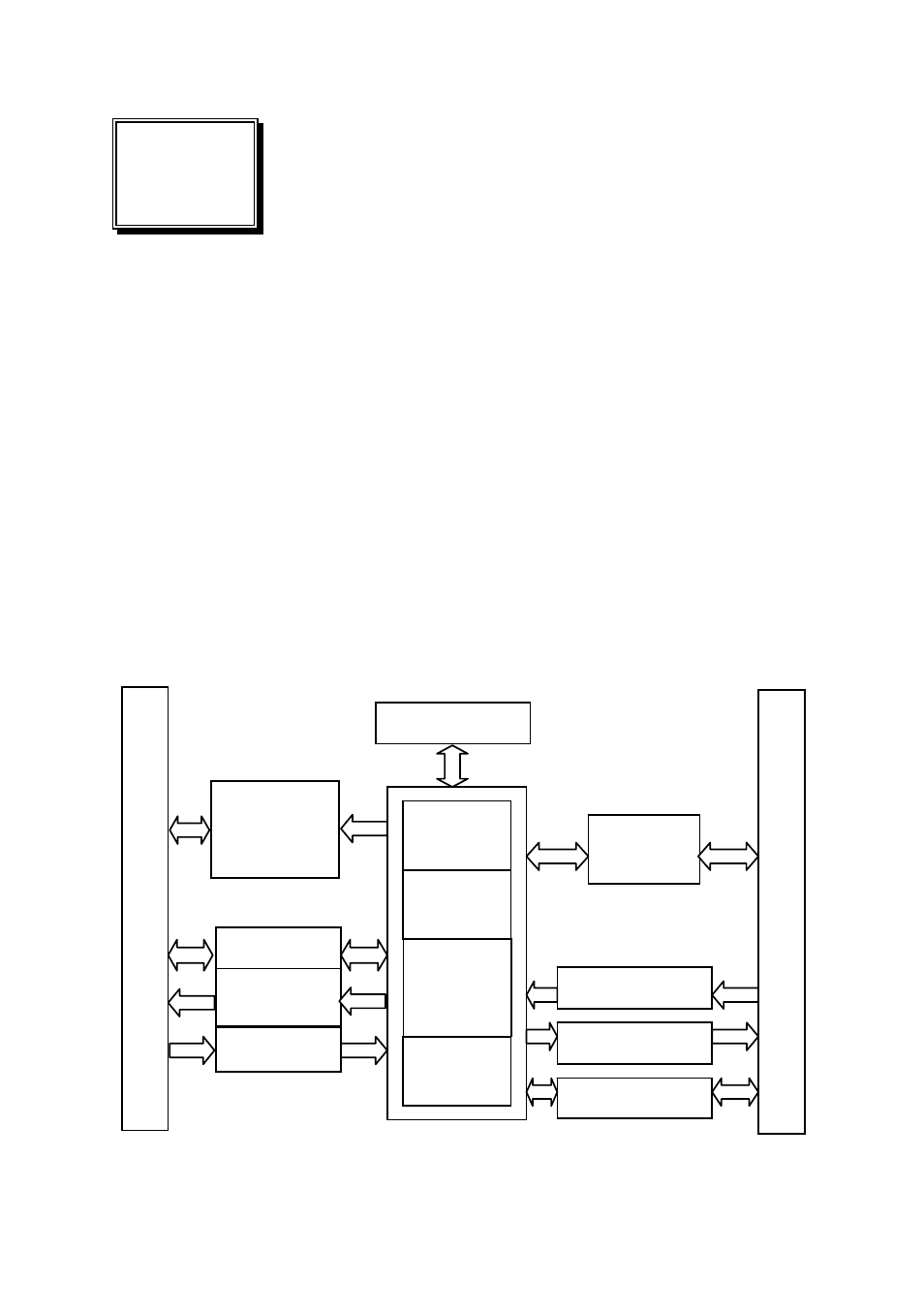
4.1 Hardware Block Diagram
The ADLINK PXI Switch Module features an onboard FPGA for relay switching
control, trigger control, scanlist storage and sequencing. The PXI triggering and
synchronization functions, such as Star Trigger and Trigger Bus are also
supported. In addition to the Trigger In and Scanner Advanced signals for
external instruments handshaking, the switch module provides eight channels
of programmable digital I/O interface to facilitate general purpose control
applications.
To make full use of the flexible trigger and signaling system on the PXI platform,
the switch module has a built-in signal routing matrix that can exchange signals
between front panel digital I/O, Star Trigger, and Trigger Bus.
Figure 3: Hardware Block Diagram
Relay
Scan Memory
PXI
Interface
Front Connector
PXI Connector
Trigger-in
Scan-
Advance
PXI Trigger Bus
Star Trigger Out
Star Trigger In
DIO
Relay
Control
Timing
Control
Trigger
Control
Signal
Routing
Matrix
