2 analog output status register, 3 current output and range control, Analog output status register – ADLINK PCM-6308V+ User Manual
Page 35: Current output and range control, Figure 4-1: current output circuit
Operation Theory
25
4.2 Analog Output Status Register
The DAC uses a series bus architecture hence there is a delay in
the output of the digital value. The data transfer time for every DA
data write takes 13
µ
s, therefore the software driver must wait for
13
µ
s before sending another set of data to any analog output port.
While the DA value is sending, the Data_Send bit is ‘H’. The soft-
ware driver should check this bit before writing any data to the out-
put port. This register is read only.
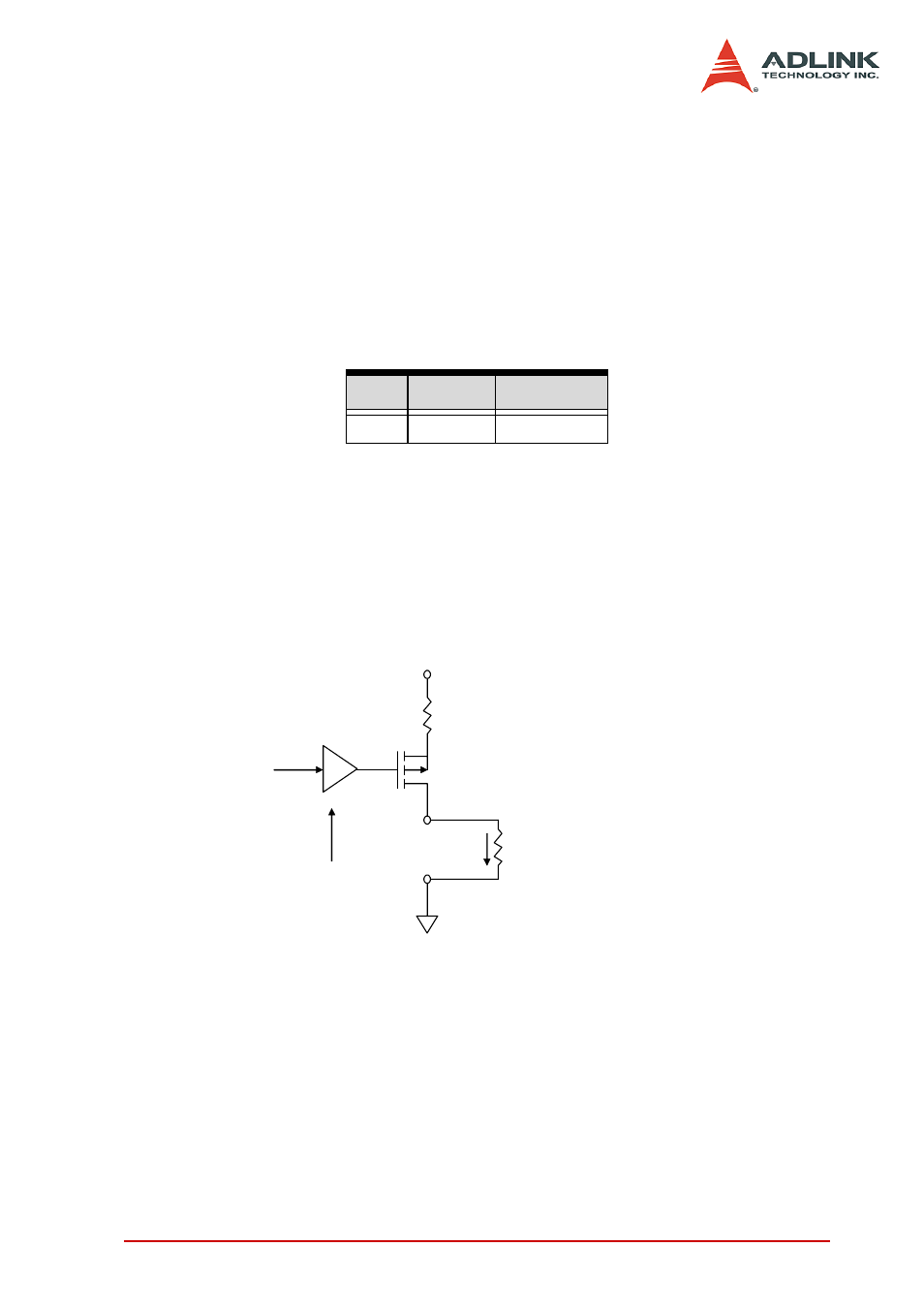
4.3 Current Output and Range Control
A precision voltage-to-current converter XTR110 implements the
current output. The current output channel n (An) is control by the
voltage of channel n (Vn). A block diagram of the current output
channels is shown in the figure below:
Figure 4-1: Current Output Circuit
The PCI-6308A provides an on board +15V power supply. Each
current output channel is a current source, which is controlled by
the voltage of the corresponding voltage output channel. For
Base D16~D1
D0
0x00
X
Data_Send
XTR110
50 Ohm
On Board +15V
Vn
An
External Load
(Resister R
L
= 250 Ohm typical)
A.GND
Io
Current Output
Range Control