4 advanced chipset setup – Acrosser AR-B1790 User Manual
Page 28

AR-B1790 User’s Guide
28
Boot to OS/2
When using the OS/2 operating system, you need to Yes this option otherwise leave this on the setup default of
No.
L1 Cache
This option specifies the caching algorithm used for L1 internal cache memory.
L2 Cache
This option specifies the caching algorithm used for L2 secondary (external) cache memory.
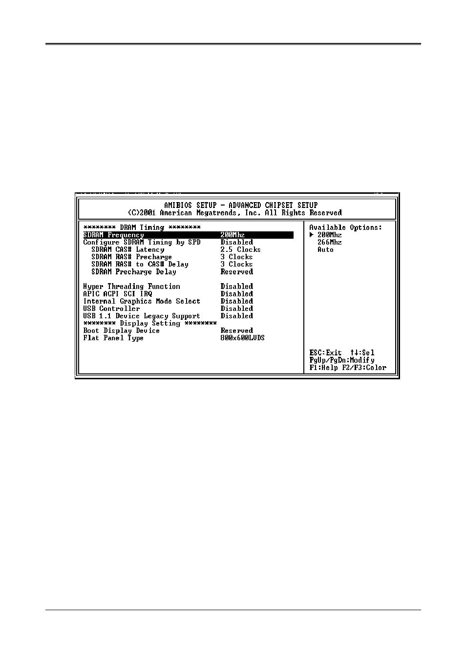
5.4 ADVANCED CHIPSET SETUP
This option controls the configuration of the board’s chipset. Control keys for this screen are the same as for the
previous screen.
Advanced Chipset Setup
DRAM Frequency
PC-200 means the memory bus is running at 200MHz. PC-266 means the memory bus is running at 266MHz.
The Choice: 200Mhz, 266Mhz
Configure SDRAM Timing by SPD
SPD is the abbreviation Serial Presence Detect. SPD takes accord the chip types, capacity, timing, voltage data.
The system can auto adjust memory according to the data to reach the best situation.
The Choice: Enabled, Disabled
CAS# Latency
This controls the timing delay (in clock cycles) before SDRAM starts a read command after receiving it. Settings:
1.5, 2, 2.5, 3 (clocks). 1.5 (clocks) increases the system performance the most while 3 (clocks) provides the most
stable performance.
RAS# to CAS# Delay
This field allows you to set the number of cycles for a timing delay
Precharge Delay
The field specifies the idle cycles before precharge an idle bank. Settings: 7, 6, 5 (clocks).
