Acrosser AR-B1551 User Manual
Page 11

AR-B1550 User’s Guide
9
required to handle the communications link.
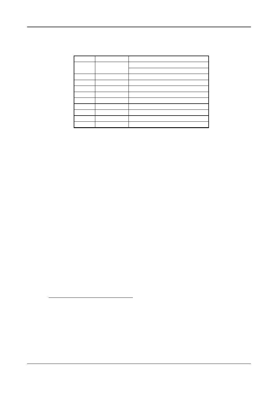
The following table is a summary of each ACE accessible register
DLAB Port
Address
Register
Receiver buffer (read)
0
base + 0
Transmitter holding register (write)
0
base + 1
Interrupt enable
X
base + 2
Interrupt identification (read only)
X
base + 3
Line control
X
base + 4
MODEM control
X
base + 5
Line status
X
base + 6
MODEM status
X
base + 7
Scratched register
1
base + 0
Divisor latch (least significant byte)
1
base + 1
Divisor latch (most significant byte)
ACE Accessible Registers
(1) Receiver Buffer Register (RBR)
Bit 0-7: Received data byte (Read Only)
(2) Transmitter Holding Register (THR)
Bit 0-7: Transmitter holding data byte (Write Only)
(3) Interrupt Enable Register (IER)
Bit 0: Enable Received Data Available Interrupt (ERBFI)
Bit 1: Enable Transmitter Holding Empty Interrupt (ETBEI)
Bit 2: Enable Receiver Line Status Interrupt (ELSI)
Bit 3: Enable MODEM Status Interrupt (EDSSI)
Bit 4: Must be 0
Bit 5: Must be 0
Bit 6: Must be 0
Bit 7: Must be 0
(4) Interrupt Identification Register (IIR)
Bit 0: “0” if Interrupt Pending
Bit 1: Interrupt ID Bit 0
Bit 2: Interrupt ID Bit 1
Bit 3: Must be 0
Bit 4: Must be 0
Bit 5: Must be 0
Bit 6: Must be 0
Bit 7: Must be 0
(5) Line Control Register (LCR)
Bit 0: Word Length Select Bit 0 (WLS0)
Bit 1: Word Length Select Bit 1 (WLS1)
Bit 2: Number of Stop Bit (STB)
Bit 3: Parity Enable (PEN)
Bit 4: Even Parity Select (EPS)
Bit 5: Stick Parity
Bit 6: Set Break
Bit 7: Divisor Latch Access Bit (DLAB)
WLS1 WLS0
Word
Length
0 0
5
Bits
0 1
6
Bits
1 0
7
Bits
1 1
8
Bits
