Sutherland PhonoBlock User Manual
Page 6

Some are small. For instance, if the front panel logo were simply silk-screened ink, sitting on the sur-
face of the panel it would, over the years, rub off. It is actually a black dye anodized INTO the alumi-
num. You can see and even feel the difference.
Some are big. The base of the PhonoBlock is laser machined 12 gage cold rolled steel. That’s about
1/8” thick. That substantial platform is protected with baked on epoxy power coat.
Feet are custom machined from Delrin with rubberized cork inserts.
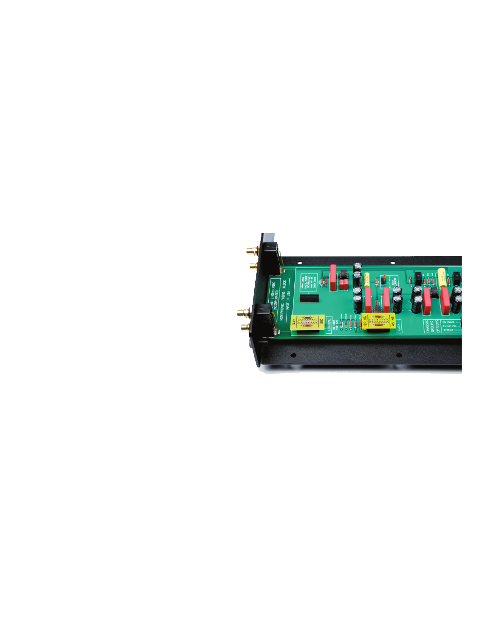
The theme of robust construction is also evident in the circuit boards. Fiberglass FR-4 is a well estab-
lished, top quality choice for circuit board material. However, what you will see in the PhonoBlock is
over the top. At 1/8” thickness, PhonoBlock circuit boards are twice as thick as normally seen. Indi-
vidual parts are anchored from any mechanical movement.
PRINTED CIRCUIT DIELECTRIC:
Anytime two conductors are at a different voltage
potential, there is an electric field generated be-
tween them. The dielectric (the insulation between
conductors) within that field become involved in
charge storage. If not carefully considered, that
extra charge storage can time smear details of
a musical signal. Circuit board material is a
dielectric. With normal double-sided construc-
tion, there are copper conductors on each side
of the board. Unintentionally, a new capacitor is
introduced into the circuit, formed by top surface
copper, bottom surface copper and the circuit board
dielectric sandwiched between the two. It is NOT the
quality of capacitor we want to have
in a high-end signal path. Some manufactures make the situation even worse by going to multi-layer
boards in the analog audio sections. Instead of two layers of copper, there are four or more layers of
copper. Even worse than that, the dielectric between layers is much thinner and the undesired capaci-
tive effect is inversely proportional to thickness. At best, some manufactures make small, incremental
improvements by using exotic board material.
The PhonoBlocks addresses the issue of circuit board dielectric in a novel – yet elegantly simple way.
All signal carrying conductors are on the top plane of the circuit board. There are no copper conduc-
tors on the bottom plane, opposite signal carrying regions. Thus there are no electric fields generated
between top and bottom layers. The circuit board dielectric is not exposed to electric fields and there is
no undesired storage in circuit board material. The circuit board dielectric is not improved ---------- it is
removed. It is as if a window were behind you, instead of in front of you. It is still there, but not in the
way of clarity.
