Fuctional description, Digital & analog co., ltd. (rev. 1.0) -5 – Calyx S1A0051 - FET Driver for Class-D PWM Amp User Manual
Page 5
S1A0051 FET Driver for Class-D PWM Amp
Digital & Analog Co., Ltd. (Rev. 1.0) -5-
6. FUCTIONAL DESCRIPTION
Please refer to notes on S1A0071 for more details on the Class-D Amp.
S1A0051 can be used not only in one power supply mode(+10V ~ +12V) but also in dual power
supply mode( ±5V ~ ±6V ). It can receive input signals through the Schmitt Trigger, and has a built-in
logic power supply, which makes the logic level independent of the input level when the input signal
level is different from the output signal level. S1A0051 drives inputs and outputs that have a non-
inverse relation S1A0051 drives each output that have a non-inverse relation about each input and it
has superior short propagation delay and fast rising/falling timing characteristics.
Input Interface (Schmitt Trigger)
In S1A0051, the built-in logic power supply sets the internal logic operating voltage, and the power
supply voltage range is 5.0V
0.5V for dual power supply mode. By interfacing with the Schmitt
Trigger with a hysteresis, the input is unaffected by noise.
Driver & 1/2 BIAS
Configured as CMOS, excluding totem pole output stage, to enhance switching characteristics, the
driver generates the center operating voltage (1/2 BIAS) to prevent MOS breakdown when the process
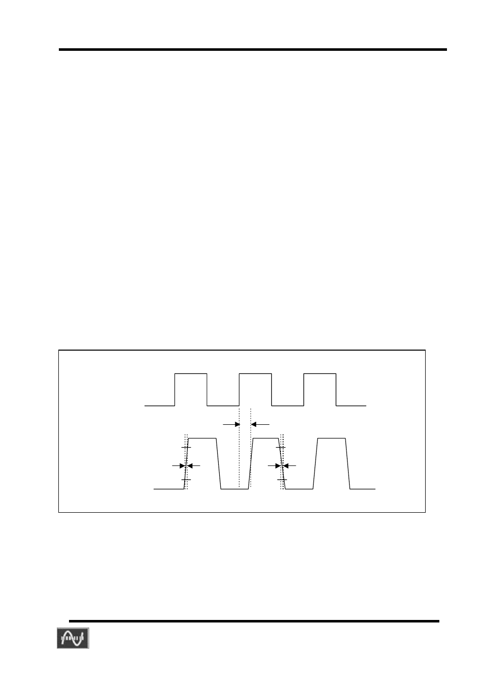
CMOS breakdown voltage BVgs is 8V. S1A0051's input/output relationship is non-inverted, which is
shown in the timing diagram in Figure. 1.
Input
Output
Td
Tf
10%
Tr
90%
90%
10%
Figure 1. Input vs. Output Timing Diagram