Product block diagram – USGlobalsat EB-5662RE User Manual
Page 3
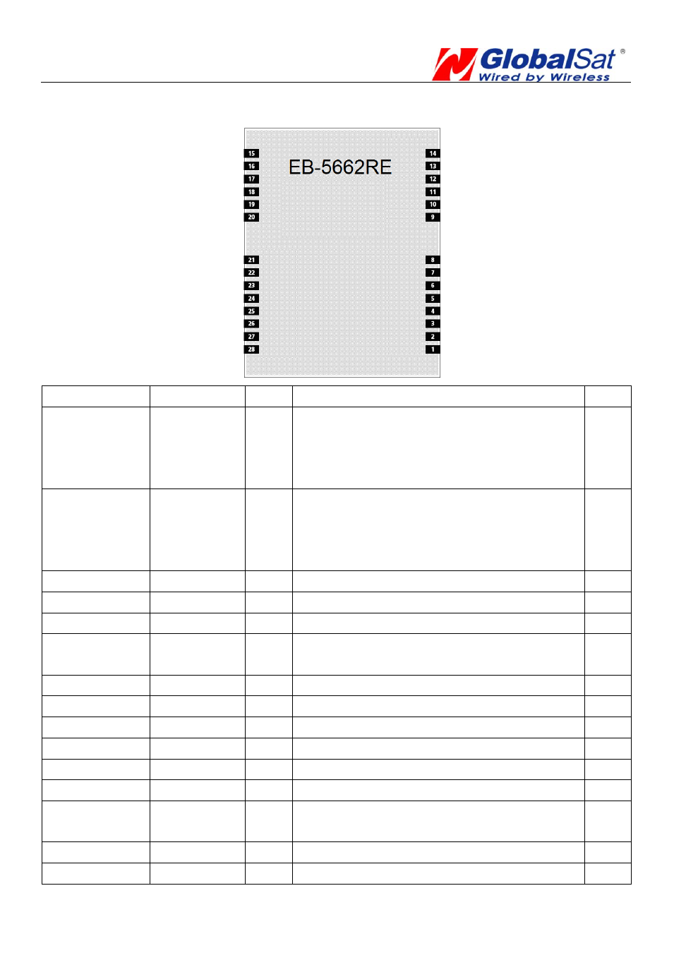
EB-5662RE
High Performance GPS Engine Board
- 3 -
Product Block Diagram
PIN Number(s) Name
Type Description
Note
3
TXD
O
This is the main transmits channel for
outputting navigation and measurement data
to user’s navigation software or user written
software. Output TTL level, 0V ~ 2.85V.
4
RXD
I
This is the main receive channel for receiving
software commands to the engine board from
SiRFDemo software or from user written
software.
1
5,6
VCC
P
Main power supply to the engine board.
7,13,14,15,17
GND
P
Ground.
8
VDD3V3OUT
O
Output voltage 3.3V
1,2,9,12,21,22,
23,24,27
NC
NC
10
RESET
I
System reset (active low)
11
VBAT
P
Backup battery supply voltage
16
RF IN
RF
GPS antenna input
18
VCC_RF
O
Supply Antenna Bias voltage (V=VCC)
19
V_ANT
I
Antenna Bias voltage
20
V-ANT_DET
I
This pin is Active Antenna detect signal input
25
ON_OFF
I
ON_OFF pin is used to command the
EB-5662RE to turn on or off
26
WAKE_UP
O
System power on, 1.8V output .
28
TIMEPULSE
O
One pulse per second output.(1PPS)