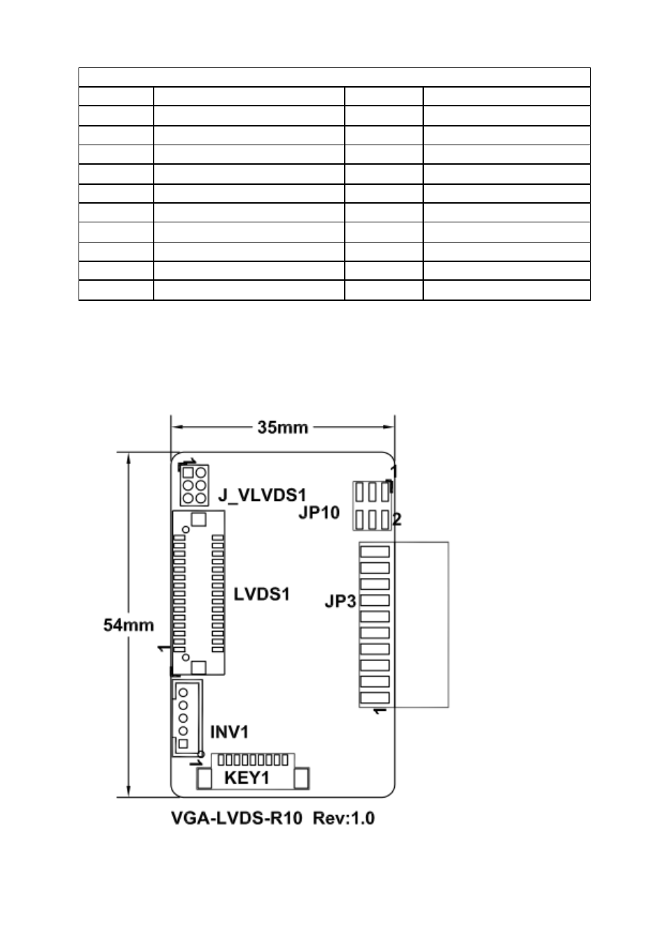
Board layout: jumper and connector locations – IEI Integration VGA-LVDS User Manual
Page 4
See also other documents in the category IEI Integration Hardware:
- SPCIE-5100DX (180 pages)
- SPCIE-C2060 v1.01 (200 pages)
- SPCIE-C2060 v2.12 (212 pages)
- SPCIE-C2160 (204 pages)
- SPCIE-C2260-i2 (217 pages)
- ROCKY-3786 v4.0 (175 pages)
- ROCKY-3786 v4.10 (147 pages)
- PCIE-Q350 v1.00 (272 pages)
- PCIE-Q350 v1.12 (250 pages)
- PCIE-Q350 v1.20 (250 pages)
- PCIE-Q350 v1.30 (213 pages)
- PCIE-Q57A (159 pages)
- PCIE-G41A2 (151 pages)
- PCIE-Q670 v1.03 (206 pages)
- PCIE-Q670 v2.00 (205 pages)
- PCIE-H610 (181 pages)
- PCIE-Q870-i2 (217 pages)
- IOWA-LX-600 (159 pages)
- PCISA-945GSE v1.01 (207 pages)
- PCISA-945GSE v1.10 (190 pages)
- PCISA-9652 v1.00 (232 pages)
- PCISA-9652 v1.01 (232 pages)
- PCISA-PV-D4251_N4551_D5251 (145 pages)
- PICOe-945GSE (197 pages)
- PICOe-GM45A (198 pages)
- PICOe-PV-D4251_N4551_D5251 v1.00 (154 pages)
- PICOe-PV-D4251_N4551_D5251 v1.10 (154 pages)
- PICOe-PV-D4251_N4551_D5251 v1.11 (155 pages)
- PICOe-B650 (156 pages)
- PICOe-HM650 (174 pages)
- HYPER-KBN (139 pages)
- SPXE-14S (3 pages)
- SPXE-9S v1.00 (5 pages)
- SPXE-9S v1.1 (6 pages)
- SPE-9S v1.00 (4 pages)
- SPE-9S v1.1 (5 pages)
- SPE-6S (3 pages)
- SPE-4S (4 pages)
- PE-6SD3 (4 pages)
- PE-6SD2 v4.0 (4 pages)
- PE-6SD2 v2.10 (3 pages)
- PE-6SD (3 pages)
- PE-6S3 v1.0 (2 pages)
- PE-6S3 v4.0 (4 pages)
- PE-6S2 (4 pages)