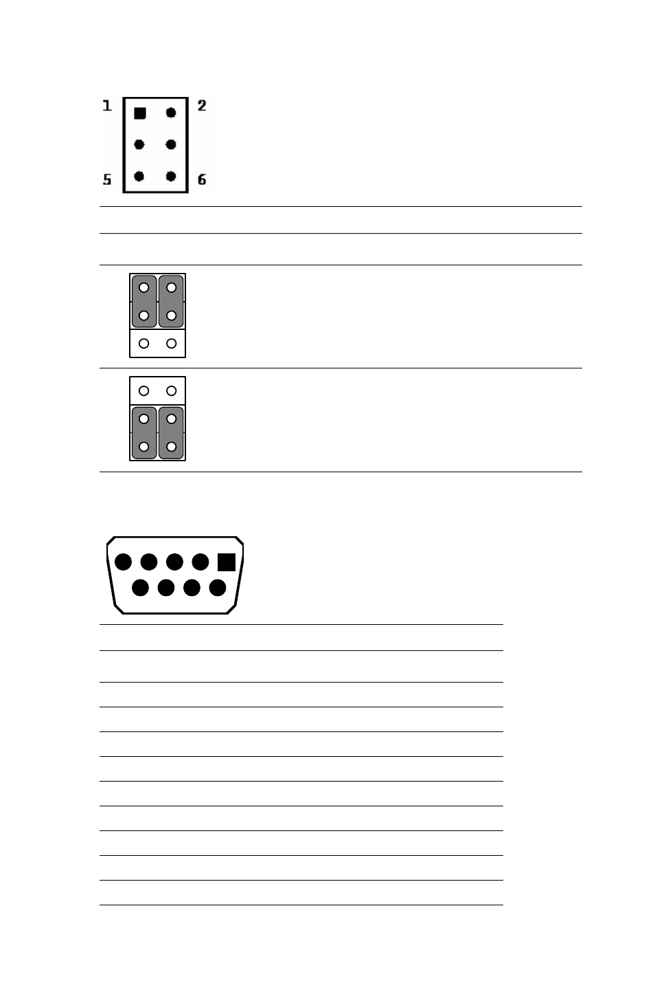
A.9.2 lvds power setting (cn17), Table a.11: cn17 configuration, A.9.3 lvds_pwr (backlight control) – Advantech UNO 2173A/AF User Manual
Page 40: Table a.12: lvds_pwr pin definition, Table a.11:cn17 configuration, Table a.12:lvds_pwr pin definition
UNO-2173A/AF User Manual
32
A.9.2 LVDS Power Setting (CN17)
A.9.3 LVDS_PWR (Backlight Control)
Table A.11: CN17 Configuration
Configuration
Function
VDD_DSUB (Pin 7 and Pin 20) of LVDS pin is +5V
VDD_DSUB (Pin 7 and Pin 20) of LVDS pin is +3.3V
Table A.12: LVDS_PWR pin definition
Pin
Signal
1
+12V (1.2A)
2
GND
3
INVERTER ENABLE
4
BRIGHTNESS (PWM)
5
+5V (1A)
6
LVDS_DDC_CLK
7
LVDS_DDC_DATE
8
GND
9
NC
2
4
6
1
3
5
2
4
6
1
3
5
1
6
5
9