Absolute maximum ratings, Electrical characteristics—5v operation – Rainbow Electronics MAX934 User Manual
Page 2
MAX931-MAX934
Ultra Low-Power, Low-Cost
Comparators with 2% Reference
2
_______________________________________________________________________________________
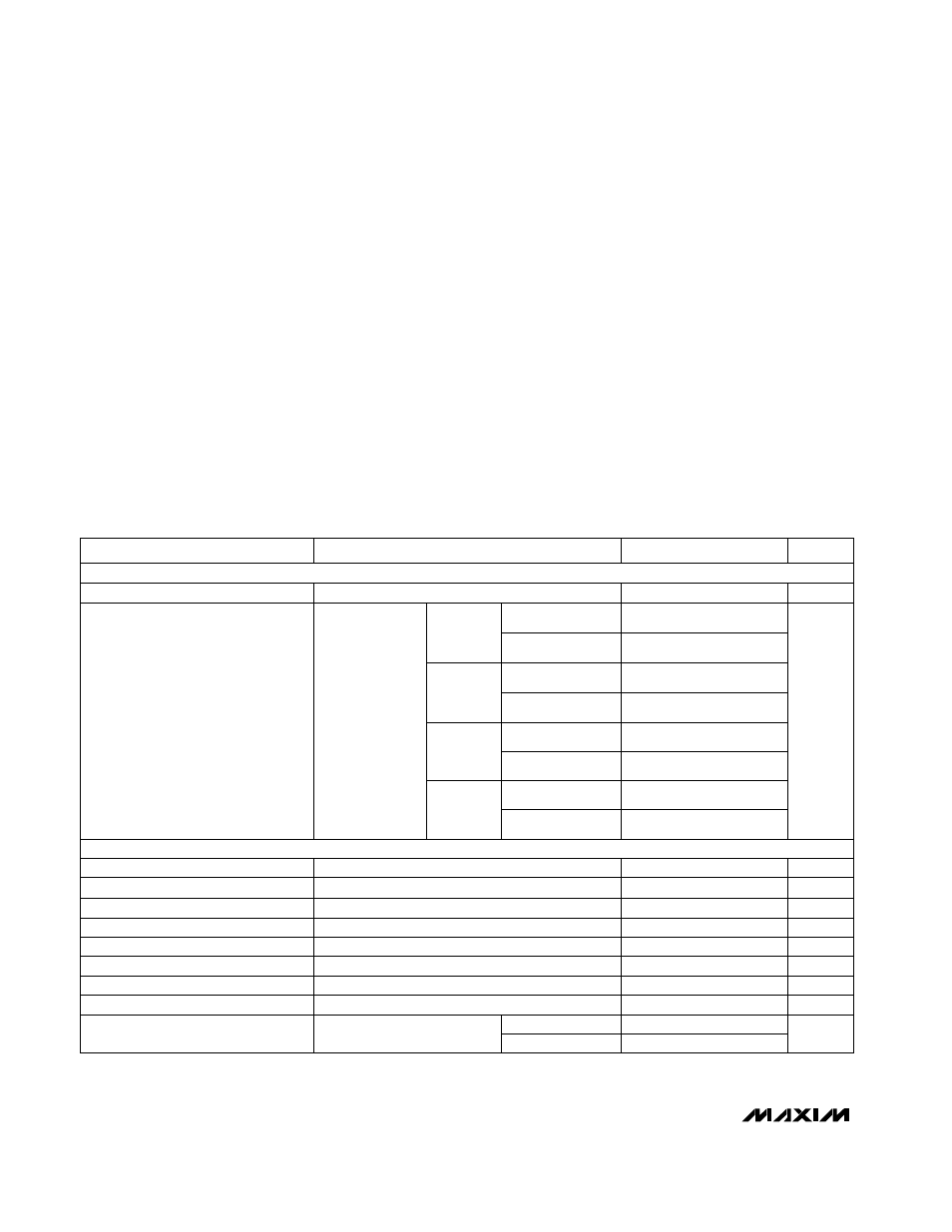
ABSOLUTE MAXIMUM RATINGS
V+ to V-, V+ to GND, GND to V-................................-0.3V, +12V
Inputs
Current, IN_+, IN_-, HYST...............................................20mA
Voltage, IN_+, IN_-, HYST................(V+ + 0.3V) to (V- – 0.3V)
Outputs
Current, REF....................................................................20mA
Current, OUT_ .................................................................50mA
Voltage, REF ....................................(V+ + 0.3V) to (V- – 0.3V)
Voltage, OUT_ (MAX931/934) .....(V+ + 0.3V) to (GND – 0.3V)
Voltage, OUT_ (MAX932/933)..........(V+ + 0.3V) to (V- – 0.3V)
OUT_ Short-Circuit Duration (V+
≤
5.5V) ...............Continuous
Continuous Power Dissipation (T
A
= +70°C)
8-Pin Plastic DIP (derate 9.09mW/°C above +70°C) ...727mW
8-Pin SO (derate 5.88mW/°C above +70°C)................471mW
8-Pin µMAX (derate 4.1mW/°C above +70°C) .............330mW
16-Pin Plastic DIP (derate 10.53mW/°C above +70°C)..842mW
16-Pin SO (derate 8.70mW/°C above +70°C) ................696mW
Operating Temperature Ranges:
MAX93_C_ _ .......................................................0°C to +70°C
MAX93_E_ _.....................................................-40°C to +85°C
Storage Temperature Range .............................-65°C to +150°C
Lead Temperature (soldering, 10sec) .............................+300°C
ELECTRICAL CHARACTERISTICS—5V Operation
(V+ = 5V, V- = GND = 0V, T
A
= T
MIN
to T
MAX
, unless otherwise noted.)
Stresses beyond those listed under “Absolute Maximum Ratings” may cause permanent damage to the device. These are stress ratings only, and functional
operation of the device at these or any other conditions beyond those indicated in the operational sections of the specifications is not implied. Exposure to
absolute maximum rating conditions for extended periods may affect device reliability.
PARAMETER
MAX933,
HYST = REF
MIN TYP MAX
UNITS
MAX934
V
V-
V+ – 1.3
MAX931,
HYST = REF
5.5
6.5
Supply Current
IN+ = IN- + 100mV
µA
Supply Voltage Range
T
A
= +25°C, 100pF load
2.5
11
V
MAX932,
HYST = REF
2.5
3.2
Input Offset Voltage
CONDITIONS
±10
mV
T
A
= +25°C
nA
Input Leakage Current (IN-, IN+)
(Note 1)
±0.01
±5
Input Leakage Current (HYST)
T
A
= +25°C
±0.02
nA
Input Common-Mode Voltage Range
V
CM
= 2.5V
Common-Mode Rejection Ratio
IN+ = IN- = 2.5V, C/E temp. ranges
MAX931, MAX932, MAX933
0.1
1.0
mV/V
Power-Supply Rejection Ratio
V- to (V+ – 1.3V)
V+ = 2.5V to 11V
100Hz to 100kHz
0.1
1.0
mV/V
Voltage Noise
MAX931, MAX932, MAX933
Overdrive = 10mV
Overdrive = 100mV
20
µV
RMS
Hysteresis Input Voltage Range
REF – 0.05
REF
V
T
A
= +25°C
12
µs
Response Time
T
A
= +25°C
4
3.1
4.5
3.1
4.5
C/E temp. ranges
4
C/E temp. ranges
6
C/E temp. ranges
6
C/E temp. ranges
8.5
POWER REQUIREMENTS
COMPARATOR